kicad-design-for-manufacture
2017-02-02 Robin Whittle
rw@firstpr.com.au This page concerns various questions of how to design PCBs in general, and with KiCad in particular, so that they both work and can be manufactured reliably and efficiently. I am not an expert in these matters. I initially wrote it in late October to mid-December 2017, while doing my first KiCad design, which was also my first SMT PCB.
(2023-09-02 mini update: I am not sure how relevant all this material is to Kicad in 2023. I haven't done any work with it since 2018. Today I updated a link to Andrew Tweddle's site, which is now https://pcbsynergy.com .)
One subject I consider is how to design footprints to match accepted standards regarding the centroid and zero rotation, and to meet other requirements, so that there is minimal need for manual effort, and minimal chances of errors, when using the .pos files (centroid files) produced by KiCad, to drive (via various other software used by the PCB assembly company) pick and place machines, for automated SMT assembly. I am not specifically considering automated through hole assembly, and I am only thinking about SMT on a single side for now.
Another perplexing problem I tried to solve (so far, I think, with success) is how to define the pads so they will work reliably with reflow soldering, while also being suitable for hand soldering for assembly, modification and repair.
I describe, in several sections below, how I made SMT footprints for my footprint library, primarily by using the freely available Windows program Library Expert LITE from pcblibraries.com, followed by some manual (and potentially automated) editing of the resulting footprint file. The editing achieves some things which differ from what is allowed by the KiCad Library Convention (KLC) approach to footprints, and from what would be achieved if I simply imported into my library (via Footprint Editor) the files exported by Library Expert Lite. (Some of these are based on how Mars_Warrior, writing on the KiCad.info forum, describes his way of designing PCBs.)
- The F.SilkS layer is used, as is conventional, for the reference of the component.
- Instead of using the F.Fab layer for the component outline and value, I use it for the component outline and reference.
- I use the Eco1.User layer to show the component outline and value.
- Library
Expert Lite creates footprints with SMT pads as rounded
rectangles and many other details which are compliant with the
forthcoming IPC-7351C standard. The typically long and detailed
names it creates for footprints are also compliant with that standard
and I frequently use these names - perhaps with some extra characters
for something more easily recognised by mortals -for my footprint
names. This is different from the KLC approach to naming.
- I change the size and line width of the text on these three
layers so it is all quite small: 0.80mm x 0.80mm with 0.15mm line
width. This is as small as my PCB manufacturer recommends for the
silkscreen layer. For some or many components in the
finished PCB design I will want the final text on F.SilkS and perhaps on F.Fab and Eco1.User
to be bigger than this, with thicker lines. I will change these
sizes manually as I design the circuit board. I would rather
start with small text since it clutters things less than larger text.
- In December 2017, no official release of KiCad supports rounded
rectangle pads, so when Library Expert Lite exports a footprint in
KiCad format, the pads are specified as ordinary rectangles. With
a text editor (or in the future perhaps a program to do the same thing)
it is reasonably easy to alter the footprint file to make all desired
rectangular pads into rounded rectangles, before importing it into
Footprint Editor, which I use to save the footprint to my
library. It is also possible to make these changes manually in
Footprint Editor.
- Although this does not affect footprints, my approach to PCB design involves using the Eco2.User layer
for lines depicting where I want the board edges to be routed
(milled). These lines and text on this layer will be in one of
the Gerber files I send to my PCB manufacturer. I do not use the Edge.Cuts layer since, according to the Pcbnew manual, any text on this layer also appears on other layers.
The final section consists of links and notes on other aspects of designing PCBs to ensure reliable and efficient manufacture of the board itself and the complete assembly of all SMT components.
Please see the parent directory for other pages I have written about how I use KiCad: ../
There may be discussion of this page on the Kicad.Info forum:
Contents
| #footprints |
01 -
Footprint centroids and zero rotation, including how to make KiCad
footprints to IPC-7351 standards manually, with Footprint Editor,
without using a standards document, and also how to make them with the
freely available Library Expert Lite, export them to KiCad and fix them
up a little before placing them in a library |
| #footprintnames |
02 - Systematic approaches to naming footprints, based on IPC-7351C |
| #initzerorotation | 03 - Initial zero rotation for SMT components: IPC-7351C Level A or B? |
| #schemsymb | 04 - Schematic symbol names |
| #validating | 05 - Validating and fine-tuning the BoM and .pos (centroid) files against the Gerber and drill files, including with VisualPlace |
| #footprintnotes |
06 - Some notes on making my own footprints |
| #pcbdfm | 07 - Various web pages, forum discussions and documents regarding PCB design for manufacture |
Some notes written on 2018-01-02, a few weeks after I wrote most of this page:
I now have some prototypes made by PCBFast
here in Australia - in Seaford, south-east of Melbourne. The boards arrived a week after I emailed them the
Gerber and drill files. The inkjet legend ("silkscreen") is a little
ragged, but that's fine. The boards were perfect in every other
respect.
Although I haven't tried automatic placement and reflow soldering of these boards, I have hand-assembled some of them. There are various mistakes, but the footprints themselves, all of which were generated as described below by adapting the exported files of Library Expert, all look good. I used a late November Windows nightly of KiCad, which supports rounded rectangle pads, which the current release doesn't. KiCad version 5 will support rounded rectangle pads.
Thanks to the KiCad developers and PCBLibraries.com for the tools which enabled my first surface mount PCB design to be, as far as I know, a complete success (except for my own mistakes)!
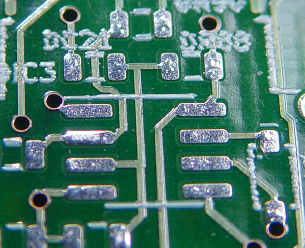
The via at the end of the diode's pad (lower right) is my mistake. The soldermask clearance (Dimensions > Pad to mask clearance > Soldermask clearance) was set to 0.125mm, according to PCBFast's recommendation, but my impression is that this value should be reduced. Note the weedy little little polarity line of the diode on the right, which is barely visible at the edge of the solder resist.
The main text of this web page has not been updated to reflect everything I know now that I have the physical boards. Nor have my libraries, which you can grab here and use as you wish:
Some things I learned were:
- The polarity line on the diodes needs to be at least twice as
thick, and moved away from the pad a little. In these prototype PCBs
the line was a single set of inkjet dots, and these sometimes fell
partially into the area lacking soldermask, which meant they did not
exist at all on these boards. Also, the errors inherent in the inkjet
process scattered the dots from the straight row they should be, so a
thicker line, hopefully producing a line two dots wide, would be better.
Hopefully the production boards, which are made in China, will use actual silkscreen for the white legend, but I have not confirmed this. (PCBFast is one of the two remaining PCB manufacturers in Australia. The other is http://www.lintek.com.au in Queanbeyan, NSW. Lintek do beautiful work, including with exotic PTFE microwave materials, and consequently do a lot of jobs for overseas customers. PCBFast used to be a full scale manufacturer, but now they make prototypes and have their quantity production done in China. My experience with PCBFast recently and with the last batch of Devil Fish boards has been 100% positive.)
- When I wrote the material below, I used three digit
numbers for resistor values, such as 223 and 104, thinking that the
actual resistors on the PCB would have these numbers printed on
them. Then I learned three things to my surprise: Firstly,
my SMT resistor book (which had 5% 0805 resistors printed like this)
did not have all the the E12 value range I assumed it had (1.0, 1.2,
1.5, 1.8, 2.2, 2.7, 3.3, 3.9, 4.7, 5.6, 6.8, 7.5, 8.2) - and I couldn't
find any on eBay which did. Secondly, many 0805 resistors from
element14 or Mouser have no markings at all. Thirdly, those which
do have markings are almost always 1% resistors and part of a much
finer range of values than the E12 range, so they have four digit
markings: 2204 and 1003.
So I will revise schematics to have 4 digit resistor numbers in the PCBValue field and these will appear in the print-out from the ECO1.User layer. (Printed by exporting to SVG and then opening and printing with Inkscape.) This will solve a pesky problem in my current three digit arrangement - capacitors with numbers such as 104 (0.1uF) being visibly indistinguishable on this layer from resistors with a 100k value.
- I should alter the footprints for the smaller SMT components, which have a small square on the ECO1.User layer, to use 0.4;0.4;0.1 text for this layer. This will enable three or four digits to fit inside the square.
This should work well if I have these value text items (mainly from the schematic's PCBValue fields) printed on the same piece of paper as the F.SilkS layer, since those items are outside the outline of the component. This can be done by two separate SVG exports, one for each layer, in black, and then by importing both into Inkscape, one at a time, changing their colours, and placing each layer's set of lines and characters one on top of the other in a third Inkscape document, which can then be printed:
This is with the 3 digit resistor values using text size 0.6; 0.6; 1.2. The diode uses 0.4; 0.4; 0.1. The printer is a 600DPI LED Brother HL-3170CDW. Apart from some colour registration errors, it produces an exceedingly crisp image.
I will likewise reconsider footprint library text sizes for the F.Fab layer, so they could generally fit into the boxes like this, for a separate print-out of references to help the PCB assembly people. For now I haven't worked on the placement or size of the F.Fab layer text.
In what follows I did not consider a significant addition to the various KiCad libraries which are made available by various designers, and programmers who automatically generate such libraries (of footprints at least) - Digi-Key's schematic symbol and PCB footprint library for KiCad:
(This was in November or early
December 2017 - this forum software doesn't seem to have concrete dates
and times for messages. The forum software frustrates my attempts
to treat a discussion as a concrete thing which can be printed.
Messages appear or are hidden according to processes beyond my
understanding.)
I haven't looked at these closely, but this is clearly a great addition to KiCad. On 2017-12-02 I made these text files listing the names of the symbols and footprints:
(The first of these was made with FileLocator Pro, the free version of which is Agent Ransack. These programs have all sorts of uses for searching for text in multiple files, directories of files etc.)
#footprints
01 - Footprint centroids and zero rotation , including how to make KiCad footprints to IPC-7351 standards manually, with Footprint Editor, without using a standards document, and also how to make them with the freely available Library Expert Lite, export them to KiCad and fix them up a little before placing them in a library
I don't have a clear idea how SMT PCB assemblers
program their pick and place machines (but see my notes on VisualPlace and NPI software below), but I want to design all the
footprints in my library so that my PCB
designs and resulting files will be as easy as possible to use for
setting up the automated assembly process.
In order to reduce manual effort and potential problems in the automated SMT assembly process, I need to make the correct choices in these regards for my schematic and footprint libraries, including:
If you think this page is in some way authoritative or a complete solution to the challenges of making footprints, please take a look at well informed people with much more experience than I have discussing this field, such as:
I think found this discussion and document extremely informative and I suggest you read them fully if you are at all interested in KiCad footprint libraries. The discussion is in a forum with characteristics I found annoying . We have to click on links to see all the replies. I found no way of printing the whole thing, and some replies seem to be repeated. Still, I think it is worth reading all the replies and following quite a few of the links.
In addition to the PCB assembly company needing the Gerber files of the whole panel of PCBs, and/or of a single PCB, they will need:
The complete design must also include, for each component (or at least each SMT component) an outline on the front (top) courtyard layer F.Crtyd, since I am only planning on components on the top (AKA front) side. This is needed when manually placing the components in the PCB design so their courtyards do not overlap.
All these things need to be considered when creating footprints for my library. Then, from the industry standard pin numbers/names (3, A, CE or whatever) of these footprints, I can create matching schematic components ("schematic symbols" is also a better term) with pin numbers/names to match these footprints.
KiCad is intended by its designers to support a schematic symbol library which does not normally specify a single footprint for each symbol (though there is a field in each symbol for doing so), but leaves it open, perhaps with some guidance by way of filters, for which footprints will be chosen once the schematic is complete and it is time to create a PCB design. I, and many others, have footprints set in at least some of the schematic library components. I design the schematic in sections, with each section being implemented in the PCB design, rather than leaving the PCB design to a completely separate stage after the schematic is supposedly finished. This process involves revisions to already existing sections of the schematic and PCB design. For instance, the choice of which sub-section of dual and quad op-amps to use, or sections within a multi-gate logic chip, depend on how we lay out the PCB. Likewise the assignment of actual firmware-supported functions to particular pins of a microcontroller may depend on the PCB layout.
A list of file types within KiCad is in the main (small) KiCad manual, section 1.2:
I am not sure if there is a formal specification for the format of the .pos file, or whether the format is specified somewhere outside the KiCad project due to it being some kind of industry standard. It seems that the KiCad .pos file is an instance of a more general concept, which is not specific to KiCad or any other system: a centroid file AKA centroid data. Pick-and-place file, PnP file or P&P file are terms for the same or a similar concept. Googling these terms finds lots of pages, including this file describing a particular assembly company's specification for a centroid file:
The details of such a file, supplied to the assembler, would vary considerably depending on whether it was for a single instance of a finished PCB, or for an entire panel (AKA array) of finished PCBs which is actually manufactured and assembled as a single panel. The centroid file only concerns components which will be automatically placed on the board, so for me this is just the SMT components.
Searching for recent KiCad .pos files on the Web (Printed by Pcbnew version kicad 4.0.7) I found no files, but for 4.0.5, here is an example of a KiCad .pos file. The angles are counter-clockwise and the centroid locations are in millimetres, relative to some reference point, which should be the same as the reference point for the Gerber files (or at least this would be the most convenient arrangement for running VisualPlace).
When my first PCB design is finished, I will check the resulting BoM and .pos files with the awesome free (as in beer, not open-source) Windows program VisualPlace from CompuPhase in the Netherlands:
In order to reduce manual effort and potential problems in the automated SMT assembly process, I need to make the correct choices in these regards for my schematic and footprint libraries, including:
- The naming of pins needs to be the same as is expected by people
and software, based on various accepted standards. For
instance, the numbering of the positive pin of an electrically
polarized electrolytic capacitor - should it be 1, 2 or something else?
It certainly needs to match the numbering of pins (or pads for SMT) in
the corresponding one or more schematic symbols in my library.
- The naming, numbering or whatever of pads/pins in the footprint
library needs to conform as noted above to expectations by people and
software, not least VisualPlace, which I will be using to check my .pos and BoM (Bill of Materials) files.
- When I define a footprint in my library, it has within it an origin or
centroid - wherever in the footprint both X and Y are zero. The
footprint's rotational orientation in the library is important, since
it will be rotated by some angle, perhaps zero, when placed in the
PCB design, and this rotational angle will be output in the .pos file
to be used (after various processes and checks) to tell the
PCB assembly company's pick-and-place machine how to rotate a component it picks up from a
tape (or tray, or tube feeder) before placing it on the PCB.
I need to get the location of this centroid, and the initial orientation (rotation) of the footprint right, which means complying with accepted industry standards - the forthcoming IPC-7351C.
- I also need to design the precise footprint details, the exact
shapes of pads, choices of holes (for through-hole parts) etc. so they
work reliably in terms of reflow soldering (SMT only) and manual soldering (through hole parts).
This involves considerations of the overall density of component
placement in the final PCB, how easy it would be to manually desolder
and resolder components, how easy it would be to use test probes
etc. Fortunately there is guidance on this and I generally choose
to use the guidance for "medium" density, AKA "median" or "normal"
density.
- The names of footprints involve some choices. I could use plain imperial names such as 0805and
not bother with their metric equivalent. This seems to be
what most people do, but I think that using these alone is not the way
to build a library which I will use for the next few decades.
Below I link to documents which lay out an elaborate scheme for naming
footprints. In practice, I use Library Expert Lite's names.
- I want to use footprints with rounded rectangle pads for SMT, so I am using a development version (nightly compilation) of KiCad, rather than the current (October 2017) release version 4.0.7. For some of what follows I used a 2017-09-19 development version. Then I used later ones, such as from 2017-11-01. These are all Windows nightlies: http://downloads.kicad-pcb.org/windows/nightly/
If you think this page is in some way authoritative or a complete solution to the challenges of making footprints, please take a look at well informed people with much more experience than I have discussing this field, such as:
#thread00
https://forum.kicad.info/t/why-are-the-kicad-library-conventions-non-ipc-compliant/3678/
#pcblib2013
http://www.pcblibraries.com/downloads/Guidelines%21PCB_Design_Optimization_Starts_in_the_CAD_Library.asp
https://forum.kicad.info/t/why-are-the-kicad-library-conventions-non-ipc-compliant/3678/
#pcblib2013
http://www.pcblibraries.com/downloads/Guidelines%21PCB_Design_Optimization_Starts_in_the_CAD_Library.asp
I think found this discussion and document extremely informative and I suggest you read them fully if you are at all interested in KiCad footprint libraries. The discussion is in a forum with characteristics I found annoying . We have to click on links to see all the replies. I found no way of printing the whole thing, and some replies seem to be repeated. Still, I think it is worth reading all the replies and following quite a few of the links.
In addition to the PCB assembly company needing the Gerber files of the whole panel of PCBs, and/or of a single PCB, they will need:
- A Bill of Materials (BoM) file. See my notes on other pages here ../ about generating BoM files in various forms.
- The .pos file produced by KiCad, or some derivatives of this file which is more suitable for them.
- A PDF of the F.Fab layer of
the PCB design. At least for the SMT components, this will
contain an outline of each component's package, and within it the
reference designator (C10, R56
etc.)
of each component. They will use this to index into the BoM for
all other details, such as the value, part number, possible part
numbers, specification (so they can decide whether one of their
in-stock components is suitable) etc. They might also want a PDF of a the Eco1.User layer, which has these outlines and the value of each SMT component - and probably most through hole components too.
The complete design must also include, for each component (or at least each SMT component) an outline on the front (top) courtyard layer F.Crtyd, since I am only planning on components on the top (AKA front) side. This is needed when manually placing the components in the PCB design so their courtyards do not overlap.
All these things need to be considered when creating footprints for my library. Then, from the industry standard pin numbers/names (3, A, CE or whatever) of these footprints, I can create matching schematic components ("schematic symbols" is also a better term) with pin numbers/names to match these footprints.
KiCad is intended by its designers to support a schematic symbol library which does not normally specify a single footprint for each symbol (though there is a field in each symbol for doing so), but leaves it open, perhaps with some guidance by way of filters, for which footprints will be chosen once the schematic is complete and it is time to create a PCB design. I, and many others, have footprints set in at least some of the schematic library components. I design the schematic in sections, with each section being implemented in the PCB design, rather than leaving the PCB design to a completely separate stage after the schematic is supposedly finished. This process involves revisions to already existing sections of the schematic and PCB design. For instance, the choice of which sub-section of dual and quad op-amps to use, or sections within a multi-gate logic chip, depend on how we lay out the PCB. Likewise the assignment of actual firmware-supported functions to particular pins of a microcontroller may depend on the PCB layout.
A list of file types within KiCad is in the main (small) KiCad manual, section 1.2:
I am not sure if there is a formal specification for the format of the .pos file, or whether the format is specified somewhere outside the KiCad project due to it being some kind of industry standard. It seems that the KiCad .pos file is an instance of a more general concept, which is not specific to KiCad or any other system: a centroid file AKA centroid data. Pick-and-place file, PnP file or P&P file are terms for the same or a similar concept. Googling these terms finds lots of pages, including this file describing a particular assembly company's specification for a centroid file:
The details of such a file, supplied to the assembler, would vary considerably depending on whether it was for a single instance of a finished PCB, or for an entire panel (AKA array) of finished PCBs which is actually manufactured and assembled as a single panel. The centroid file only concerns components which will be automatically placed on the board, so for me this is just the SMT components.
Searching for recent KiCad .pos files on the Web (Printed by Pcbnew version kicad 4.0.7) I found no files, but for 4.0.5, here is an example of a KiCad .pos file. The angles are counter-clockwise and the centroid locations are in millimetres, relative to some reference point, which should be the same as the reference point for the Gerber files (or at least this would be the most convenient arrangement for running VisualPlace).
### Module positions - created on 04/10/17 16:52:49 ###
### Printed by Pcbnew version kicad 4.0.5
## Unit = mm, Angle = deg.
## Side : top
# Ref     Val                 Package                                                  PosX       PosY       Rot  Side
C1        1u                  C_0603                                               122.5000   -90.5000   90.0000  top
C2        10n                 C_0603                                               124.6505   -86.0425  270.0000  top
C3        1u                  C_0603                                               127.3500   -98.7500   90.0000  top
C4        47u                 C_1210                                               121.0000   -81.5000   90.0000  top
C5        10u                 C_0805                                               123.8250   -82.0000   90.0000  top
D1        LED_ALT             LED_0603                                             132.2070   -80.2640  180.0000  top
L1        Ferrite_Bead_Small  R_0603                                               120.5000   -90.6310   90.0000  top
P1        CONN_01X06          Pin_Header_Straight_1x06_Pitch2.54mm_SMD_Pin1Right   114.0675   -95.4630    0.0000  top
R1        1k                  R_0603                                               124.7140   -88.9000  270.0000  top
R2        1k                  R_0603                                               128.9050   -80.2640    0.0000  top
U1        LD3985M33R          SOT-23-5                                             121.7150   -86.5670   90.0000  top
U2        4050                SO-16-N                                              122.0500  -101.8500  270.0000  top
## End
The above link also leads to free, open source programs for Windows and Linux KiCad Librarian which
enables, amongst other things, superimposed visual comparisons
between footprints in the same or different libraries, and another
program for creating drill files from KiCad projects. (However,
in October 2017, KiCad Librarian does not display the curved corners of
the rounded rectangle pads I am using.)
Here is my current thinking, in early-November 2017, based the above-mentioned document pcblib2013 and discussion thread00 and initial discussions on the KiCad mailing list early in 2016 - #thread01: https://groups.yahoo.com/neo/groups/kicad-users/conversations/topics/21460 .
As far as I can see there is a clear choice of technical standards to comply with regarding SMT component centroids and zero rotation angles - the IPC 7351x series. First, my understanding of the history behind these.
The above is a summary of the relevant standards documents, but I don't actually need a standards document to create my library footprints.
#2docs
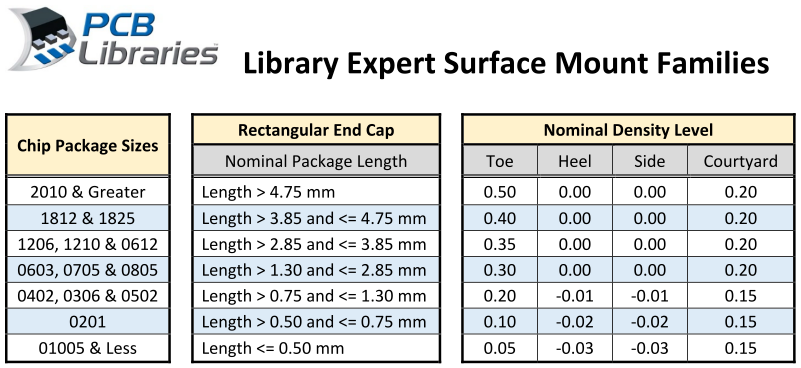
The two documents Library Expert Surface Mount Families.pdf and Library Expert Through-hole Families.pdf tell me a lot of what I need to know:

Before going any further, on 2017-10-19 I downloaded and installed the latest KiCad nightly (development version) from:
Later I installed kicad-r8665.e5c4cfc3b-x86_64.exe 01-Nov-2017
These nightlies' Footprint Editor supports rounded rectangle pads:
Next I made two attempts at making sure this 0805 (EAI imperial name) resistor footprint matches what is specified by IPC-7351 (in its current state of IPC-7351C almost being released), which is the basis of both Library Expert Through-hole Families.pdf and Library Expert Lite (as described below).
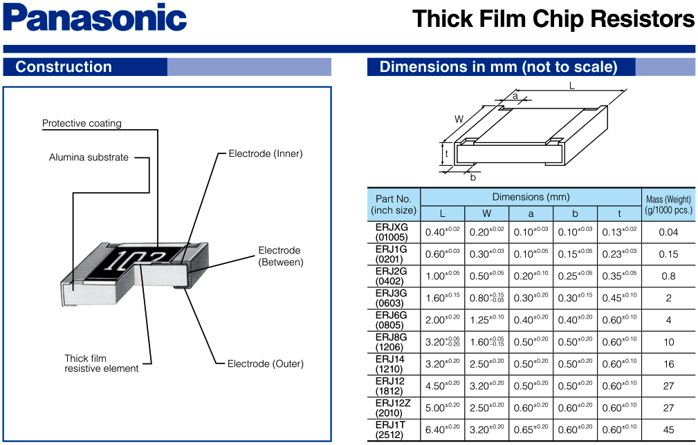
For the dimensions of the 0805 device itself, I need overall dimensions and the length (or width) of the metal contacts. The first two can be found on many websites but the third is more obscure. I looked at:
and obtained a data sheet from there: RDA0000/AOA0000C301.pdf . A table there shows the length of the metal contact in column b:
There is an example below of these change. These changes are not the same as what changes I would make to a footprint file which followed the KiCad Library Conventions (see below), since such a file is somewhat different from the file generated by Library Expert Lite.
I understand that Mars_Warrior wants the F.Fab layer to produce a drawing which a PCB assembly company can use, so that every SMT component they are going to mount has an outline and the RefDes (reference) text. From this, they can look up all the details, such as part number, value (e.g. uF and voltage, or resistance, or a range of possible part numbers, each with links to suppliers websites) in the BoM file.
I understand he wants the Eco1.User layer to produce a similar drawing, for when he is hand-assembling a board. This has the same component outlines, but has the value instead - such as a simple resistance (2K7), capacitance (334), connector part number, microcontroller part number etc. - so he can instantly see what to place in each location. I think this is primarily for SMT components which are so small and densely packed that it may not be possible to have any text for many of them on the board itself (F.SilkS) and it would generally be impossible to have values on F.SilkS in addition to the reference text, even if there was room for the reference text.
It doesn't matter much how small the text is for reference and value on the F.Fab or Eco1.User layers since these are not part of the physical circuit board. It is easy to zoom on on these when looking at the computer monitor, or print these layers on large enough pieces of paper that the text can be read. With the silkscreen layer, the text really needs to be outside the body and pins of the component, whereas this is not a restriction on F.Fab, Eco1.User or other non-physical layers. So it is possible and desirable on the F.Fab and Eco1.User layers to have the outline of the component and the text of either the reference or the value, potentially inside the outline. In principle it might be possible and desirable to have both the reference (C12 etc.) and the value (104 etc.) on the same layer, but that could be cluttered and the part numbers or values can be very long.
According to the Pcbnew manual (2017-08-24 version), page 37:
This duplication of text does not suit my needs for a layer to send to PCBFast.com.au, which has lines to describe routed (milled) edges and text regarding this and perhaps other things. In principle I could choose to put this information on Dwgs.User, but that is already in use with the outlines of the components and their terminals (at least for the above example).
On this page, the purpose of the Fabrication layers is not clearly defined:
Following Mars Warrior's example I will use Eco1.User as he does, which leaves Eco2.User for my routing (milling) and other mechanical information, which is needed by the PCB fabricator.
The way I (and I think Mars Warrior and Joan Sparky, both of whom post to the KiCad forum) want to use KiCad appears to be different from the usage pattern supported by the KiCad library standard, formally known as the KiCad Library Convention, hereafter KLC (I am referring to rev 3.0.0 on 2017-11-03):
Until early November 2017, the KLC (rev 2.0.12) was here:
Section F5.2 (2017-11-04) requires that footprints in the footprint library that the F.Fab layer have three things for each footprint:
Section F5.1 (2017-11-04) requires that footprints in the footprint library that the F.SilkS layer has only one text item things for each footprint:
Now it is time to consider the mechanism of fp_text items in footprints, in the footprint library and for footprints in a PCB design within Pcbnew, as they are automatically placed, then then manually edited. This is quite tricky since I am considering several steps:
I am also thinking about how the footprint behaves when Pcbnew loads it from my footprint library (I currently have only one) into a PCB design due to manual placement, automatic placement due to loading a netlist - and how it behaves if the footprint is already in the PCB design but is somehow updated as a result of a netlist load. (To do: when does this occur???)
My primary interest is what state the footprint file must be in before being imported into Footprint Editor. What follows is based on my understanding of the program (Windows nightlies 2017-09-19 and 2019-11-01), various forum discussions and some source code :
Here is another perfectly valid text item:
There are three types of fp_text item:
Also of potential interest is this unofficial account of KiCad file formats from the author of VisualPlace:
which states, regarding the reference and value types of fp_text item:
From this, I observe:
Broadly speaking, there are three types of footprint file I am considering:
The 2017-19 version of Library Expert Lite does not produce anything for the Eco1.User layer. As I understand its options, the component outline, fp_text reference and fp_text value for the top of the PCB are all put on whatever KiCad layer we like - and F.Fab is the default - by way of the "Assembly Outline" line in the KiCad exporter options.
My understanding (late October 2017 with Library Expert Lite 2017-19 and a KiCad nightly from 2017-09-19) is:
Here is a table regarding the graphic elements (lines, arcs or circles etc.) representing the outline of the package in the footprints of several types.
These are the layers on which the footprints in my library have graphic elements - lines, arcs and circles - listed with the usual line width and their purpose.
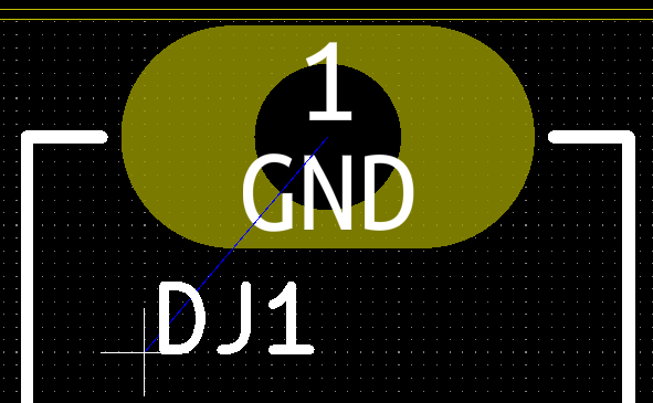
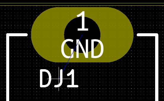
I also had to decide what arrangements my library components would have concerning where the cursor appears relative to a text item when moving it. In my PCB design I had made some such items place the cursor at the bottom left of the text, with this text in bold at the end of some fp_text items:
This suited me since I like to line up the bottom left of the text with a grid position:
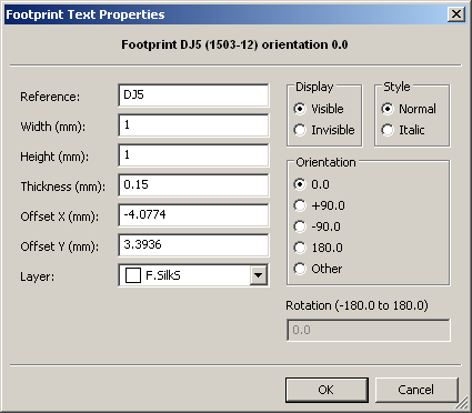
I am not sure how they got this way, since I couldn't find a way in Pcbnew of editing either the justification (left, center or right) or anything to do with top or bottom, using a Windows nightly from 2017-11-18. Editing one of these fp_text items involves a dialogue box:
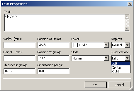
For free text items (not part of a footprint) there is a way of editing the justification to left, center or right:
Neither of these seem to provide a way of introducing bottom into this part of the PCB file.
For free text items, the "Display:" options are Normal and Mirrored. In the latter case, the PCB file contains:
I decided to change this way of working so that the cursor is (by default at least) centred both horizontally and vertically:
The reasons for this are:
This means that if I have two text items side-by-side, with differing text heights, and want the bottom edge of their characters to line up, then I will need to do some fancy manual editing or place them very finely with a 0.01mm grid, and get them at least this close - ten microns.
So I manually edited my PCB design file to get rid of all such justify constructs.
See a section below for some examples of SMT and through-hole footprints I generated using Library Expert Lite for my KiCad library. Before I could do this, I needed to sort out some other things mentioned in the following sections.
#footprintnames
Here is my current thinking, in early-November 2017, based the above-mentioned document pcblib2013 and discussion thread00 and initial discussions on the KiCad mailing list early in 2016 - #thread01: https://groups.yahoo.com/neo/groups/kicad-users/conversations/topics/21460 .
As far as I can see there is a clear choice of technical standards to comply with regarding SMT component centroids and zero rotation angles - the IPC 7351x series. First, my understanding of the history behind these.
IPC-SM-782A 1993, with amendments 1 and 2 in 1996 and 1999 respectively.
Superseded by IPC-7351.
IPC-7351 2005-02 (link) Superseded by IPC-7351A.
IPC-7351A 2007-02 (link) Superseded by IPC-7351B.
IPC-7351B 2010-01 (link) This seems to be the current (October 2017) version of the standard. However, according to a 2015-05-08 presentation by Tom Hausherr, CEO and founder of pcblibraries.com , there will be an IPC-7351C: http://www.ocipcdc.org/archive/What_is_New_in_IPC-7351C_03_11_2015.pdf and https://www.cskl.de/fileadmin/downloads/PCBLIBRARIES/Documentation/What-is-New-in-IPC-7351C_.pdf .
IPC-7351C This has not yet (2017-10-21) been finalised. Various documents about it can be found on the Web by searching for "What's new in IPC-7351C" such as #wnipc7351c https://www.cskl.de/fileadmin/downloads/PCBLIBRARIES/Documentation/What-is-New-in-IPC-7351C_.pdf . The latest news I could find on its slow progress (since 2012), and the degree to which its new contents have been incorporated into software and other documents, is this discussion #thread02, in which the last message was on 2016-11-01: https://www.pcblibraries.com/forum/ipc7351c-draft-or-release-date_topic1818.html
In the above-mentioned thread01 I mentioned some of the new features of IPC-7351C, including pads shaped as rounded rectangles. KiCad release versions cannot yet (4.0.7 in November 2017) support rounded rectangles. Such pads apparently have an advantage of greater reliability in reflow soldering.
According to this #thread03 https://github.com/KiCad/kicad-library/issues/1137 in April 2017, rounded rectangles (roundrect) will not appear in KiCad until version 5 is released, but they are supported by the nightlies (compilations of the development version of the whole KiCad project done every day, with bleeding edge code).
In thread01, regarding the "What's new" document, I wrote:
http://tinymicros.com/wiki/File:IPC-SM-782A.pdf
https://www.pcb-3d.com/wordpress/wp-content/uploads/ipc-sm-782a_amendment_1_and_2.pdf
https://www.pcb-3d.com/wordpress/wp-content/uploads/ipc-sm-782a_amendment_1_and_2.pdf
Superseded by IPC-7351.
IPC-7351 2005-02 (link) Superseded by IPC-7351A.
IPC-7351A 2007-02 (link) Superseded by IPC-7351B.
There is a document from this time,
which some people writing on PCB forums quote as one they refer
to. It is from ipc.org, the IEC and pcblibraries.com Electronic Component Zero Orientation For CAD Library Construction, available here http://ohm.bu.edu/~pbohn/... . (This is not to be confused with a standard with a similar name, most recently from 2017: IEC 61188-7-2017.)
The PDF date is 2007-11-30. It mentions a set of standards
IPC-7351 to 7359, but there's no sign of 7352 and above at ipc.org now.
This document is not a standard, but contains lots of pertinent information from the time from the relevant standards. It doesn't mention IPC-7351A.
I think that the current (October 2017) version of the information in this document can be found in the members area of pcblibraries.com, as mentioned below #2docs. These are available after a free registration.
IPC-7351B 2010-01 (link) This seems to be the current (October 2017) version of the standard. However, according to a 2015-05-08 presentation by Tom Hausherr, CEO and founder of pcblibraries.com , there will be an IPC-7351C: http://www.ocipcdc.org/archive/What_is_New_in_IPC-7351C_03_11_2015.pdf and https://www.cskl.de/fileadmin/downloads/PCBLIBRARIES/Documentation/What-is-New-in-IPC-7351C_.pdf .
IPC-7351C This has not yet (2017-10-21) been finalised. Various documents about it can be found on the Web by searching for "What's new in IPC-7351C" such as #wnipc7351c https://www.cskl.de/fileadmin/downloads/PCBLIBRARIES/Documentation/What-is-New-in-IPC-7351C_.pdf . The latest news I could find on its slow progress (since 2012), and the degree to which its new contents have been incorporated into software and other documents, is this discussion #thread02, in which the last message was on 2016-11-01: https://www.pcblibraries.com/forum/ipc7351c-draft-or-release-date_topic1818.html
In the above-mentioned thread01 I mentioned some of the new features of IPC-7351C, including pads shaped as rounded rectangles. KiCad release versions cannot yet (4.0.7 in November 2017) support rounded rectangles. Such pads apparently have an advantage of greater reliability in reflow soldering.
According to this #thread03 https://github.com/KiCad/kicad-library/issues/1137 in April 2017, rounded rectangles (roundrect) will not appear in KiCad until version 5 is released, but they are supported by the nightlies (compilations of the development version of the whole KiCad project done every day, with bleeding edge code).
In thread01, regarding the "What's new" document, I wrote:
Previously, the recommended pad shape
was "oblong" - the longer sides straight with the shorter sides being
rounded as 180 degree sections of a circle. As far as I know, this is
the same as an "oval" pad in Kicad.
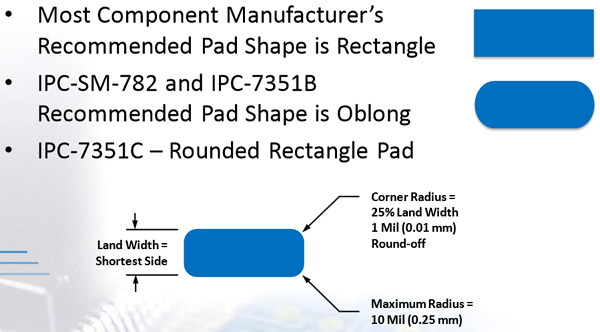
For IPC-7351C, rounded rectangle SMT pads are recommended, where the corner radius is at most 0.25mm and otherwise is 25% of the width (shortest side) of the otherwise rectangular pad. So on the shorter sides, the middle 50% is straight and the end 25% sections are 90 degree
sections of a circle.
For IPC-7351C, rounded rectangle SMT pads are recommended, where the corner radius is at most 0.25mm and otherwise is 25% of the width (shortest side) of the otherwise rectangular pad. So on the shorter sides, the middle 50% is straight and the end 25% sections are 90 degree
sections of a circle.
The above is a summary of the relevant standards documents, but I don't actually need a standards document to create my library footprints.
#2docs
The two documents Library Expert Surface Mount Families.pdf and Library Expert Through-hole Families.pdf tell me a lot of what I need to know:
- How to name pads, such as 1 and 2 for a resistor, and C and A for a diode.
- How to orient the footprint in terms of centroid and initial rotation.
- What dimensions to use for the toe, heel and side aspects of each pad, which define the PCB pad edges relative to the size of the part of the IC, resistor, etc. package which is to be soldered.
Before going any further, on 2017-10-19 I downloaded and installed the latest KiCad nightly (development version) from:
Later I installed kicad-r8665.e5c4cfc3b-x86_64.exe 01-Nov-2017
These nightlies' Footprint Editor supports rounded rectangle pads:
Next I made two attempts at making sure this 0805 (EAI imperial name) resistor footprint matches what is specified by IPC-7351 (in its current state of IPC-7351C almost being released), which is the basis of both Library Expert Through-hole Families.pdf and Library Expert Lite (as described below).
For the dimensions of the 0805 device itself, I need overall dimensions and the length (or width) of the metal contacts. The first two can be found on many websites but the third is more obscure. I looked at:
and obtained a data sheet from there: RDA0000/AOA0000C301.pdf . A table there shows the length of the metal contact in column b:
With length being X and width being Y, the figures are:
Length 2.00mm.
Width 1.25mm.
Contact length 0.40mm.
Height of contact (t) 0.60mm.
Width 1.25mm.
Contact length 0.40mm.
Height of contact (t) 0.60mm.
1 - Using Library Expert Through-hole Families.pdf #2docs
For the "normal" density level, this PDF provides the details I need to set the size and locations of the solder pads:
Page 37 shows the meaning of Toe and Heel in the context of SOIC, SOT etc. components (left diagram) and chip resistors and capacitors etc. (right diagram):
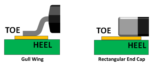
Side refers to how much further the solder pad must extend beyond the contact terminal in the directions of the arrow marked W in the Panasonic diagram.
Courtyard is defined, in IPC-7351 (2005) as:
For an 0805, the centre of the courtyard lines must be 0.2mm outside the edges of the pads.
I did some pen and paper calculations and arrived at the two pads being:
The figures in the above table were chosen for 8 size ranges of chip resistors, based on knowledge of their thickness, overall size and power dissipation. So there is no explicit mention of the thickness (t in the Panasonic table) of 0.60mm.
There may be an IPC specification for the minimum distance between any part of the component legend (AKA "silkscreen" - identifying text and/or the lines which indicate the outline of the device), but I was not sure where to look. I chose 0.15mm based on Seeed Studio's PCB Design for Manufacture 1.1 (June 2017) document (see below: #seeestudiodfm), page 7. They also state that the minimum height of text for the silkscreen is 0.60mm and the minimum thickness of the silkscreen lines, including those which make up the text, is 0.10mm.
So I designed a footprint from scratch, retaining KiCad's default 1.00mm high text with 0.15mm lines.
I won't describe this any further, because I think the second technique, using Library Expert Lite, is better. However, it does illustrate to some degree that it is possible to create footprints manually in KiCad which are technically correct, follow recognised standards for pad size, pin numbering, initial orientation etc. all based on a freely available document which is up-to-date with the current state of the art standards, the yet to be released IPC-7351C.
Side refers to how much further the solder pad must extend beyond the contact terminal in the directions of the arrow marked W in the Panasonic diagram.
Courtyard is defined, in IPC-7351 (2005) as:
The smallest rectangular area that
provides a minimum electrical and mechanical clearance (courtyard
excess) around the combined component body and land pattern boundaries.
For an 0805, the centre of the courtyard lines must be 0.2mm outside the edges of the pads.
I did some pen and paper calculations and arrived at the two pads being:
0.70mm long (X),
1.25mm wide (Y)
1.20mm (X) gap between them.
So the centres are 1.90mm (X) apart, each with an offset of 0.95mm (X) from the centroid.
The courtyard is a rectangle 2.8mm long (X) and 1.6mm wide (Y).1.25mm wide (Y)
1.20mm (X) gap between them.
So the centres are 1.90mm (X) apart, each with an offset of 0.95mm (X) from the centroid.
The figures in the above table were chosen for 8 size ranges of chip resistors, based on knowledge of their thickness, overall size and power dissipation. So there is no explicit mention of the thickness (t in the Panasonic table) of 0.60mm.
There may be an IPC specification for the minimum distance between any part of the component legend (AKA "silkscreen" - identifying text and/or the lines which indicate the outline of the device), but I was not sure where to look. I chose 0.15mm based on Seeed Studio's PCB Design for Manufacture 1.1 (June 2017) document (see below: #seeestudiodfm), page 7. They also state that the minimum height of text for the silkscreen is 0.60mm and the minimum thickness of the silkscreen lines, including those which make up the text, is 0.10mm.
So I designed a footprint from scratch, retaining KiCad's default 1.00mm high text with 0.15mm lines.
I won't describe this any further, because I think the second technique, using Library Expert Lite, is better. However, it does illustrate to some degree that it is possible to create footprints manually in KiCad which are technically correct, follow recognised standards for pad size, pin numbering, initial orientation etc. all based on a freely available document which is up-to-date with the current state of the art standards, the yet to be released IPC-7351C.
2 - Using Library Expert Lite
According to this #thread04 https://forum.kicad.info/t/kicad-pcb-library-expert/2232/8
Library Expert Lite has been able to export to KiCad since early
2016. In this thread, bobc wrote that he found the EULA for
Library Expert Lite too restrictive, but he didn't cite the text he was
referring to.
To find the EULA for a particular version of the program, use a URL such as: https://www.pcblibraries.com/Downloads/FPX!Library_Expert_2017-19_Lite.asp
with the appropriate year and version number. This is the start of a download procedure for registered users, and assuming your browser cookies reflect that fact that you are a user, you should see the EULA. Also, the EULA text is included with the zip file which includes the installer. The 2017-19 EULA starts with "Updated on May 2, 2017".
#libexpeula The only restriction I can find in the EULA regarding what we do with the footprints generated by PCB Library Expert Lite is:
The footprint file I generated, as described below, did not contain any such data. "PCB Libraries" did not appear in this file.
This page http://www.pcblibraries.com/products/compare/ indicates that the Lite version contains adware and requires an Internet connection to function. Regarding use of the Lite program, the EULA's restrictions are light compared to the single computer requirements for the paid-for Pro version:
I got the impression from bobc's comments that there was some restriction on how the footprints could be used, such as disallowing them, or any footprint derived from them, being sent to some individual or company other than the user, such as for a publicly available library. However, I see no such restriction in the current EULA.
The steps required to generate a KiCad 0805 footprint using Library Expert Lite 2017.19 are:
Here are some of the details of how I did it.
I installed Library Expert Lite (2017.19) (as it calls itself once running) which I downloaded as Library_Expert_2017-19_Lite.zip from:
This is available for Windows only and I ran it on Windows 7 Prof. 64 bit. Since this URL changes for each release, you can find the URL for the latest release from the above-mentioned version history section of the forum, or by using the above-mentioned memberdownloads.asp URL.
The Lite version's capabilities are listed at http://www.pcblibraries.com/products/compare/ in comparison to those of the Pro version for KiCad https://www.pcblibraries.com/Products/FPX/KiCad.asp which costs USD$624 for a single user perpetual license. (Though resellers may have lower prices, such as this page which may be out of date.)
Here are the actions I took to make the footprint and export it, written as instructions for you to follow.
To find the EULA for a particular version of the program, use a URL such as: https://www.pcblibraries.com/Downloads/FPX!Library_Expert_2017-19_Lite.asp
with the appropriate year and version number. This is the start of a download procedure for registered users, and assuming your browser cookies reflect that fact that you are a user, you should see the EULA. Also, the EULA text is included with the zip file which includes the installer. The 2017-19 EULA starts with "Updated on May 2, 2017".
#libexpeula The only restriction I can find in the EULA regarding what we do with the footprints generated by PCB Library Expert Lite is:
Lite
version output files may be altered, but removal or alteration of the
auto-inserted "PCB Libraries" meta data from any output files is a
violation of this Agreement.
The footprint file I generated, as described below, did not contain any such data. "PCB Libraries" did not appear in this file.
This page http://www.pcblibraries.com/products/compare/ indicates that the Lite version contains adware and requires an Internet connection to function. Regarding use of the Lite program, the EULA's restrictions are light compared to the single computer requirements for the paid-for Pro version:
LITE
and VIEWER - This Agreement entitles you to install and use the limited
"Lite" and "Viewer" versions of the Software Product on any number of
your computers. There are no restrictions on number of installations
for the "Lite" and "Viewer" versions.
I got the impression from bobc's comments that there was some restriction on how the footprints could be used, such as disallowing them, or any footprint derived from them, being sent to some individual or company other than the user, such as for a publicly available library. However, I see no such restriction in the current EULA.
The steps required to generate a KiCad 0805 footprint using Library Expert Lite 2017.19 are:
- Manually look up the dimensions of the device itself, as described above using the Panasonic data sheet.
- Manually enter these into Library Expert Lite and click various
buttons. This will produce a footprint inside the program, which
can be viewed.
- One any necessary adjustments are made, this can be exported as a KiCad.mod file.
In principle it can be saved in a library, but I had difficulty getting
KiCad's Footprint Editor to recognise the new arrival, so I exported it
to a separate directory, and imported that file into Footprint Editor.
- There are a number of things to change and clean up, such as
making SMT pads rounded rectangles.
- Then the footprint can be saved into a library.
Here are some of the details of how I did it.
I installed Library Expert Lite (2017.19) (as it calls itself once running) which I downloaded as Library_Expert_2017-19_Lite.zip from:
This is available for Windows only and I ran it on Windows 7 Prof. 64 bit. Since this URL changes for each release, you can find the URL for the latest release from the above-mentioned version history section of the forum, or by using the above-mentioned memberdownloads.asp URL.
The Lite version's capabilities are listed at http://www.pcblibraries.com/products/compare/ in comparison to those of the Pro version for KiCad https://www.pcblibraries.com/Products/FPX/KiCad.asp which costs USD$624 for a single user perpetual license. (Though resellers may have lower prices, such as this page which may be out of date.)
Here are the actions I took to make the footprint and export it, written as instructions for you to follow.
- Click the "Surface Mount" button at the top.
- From the list at the left, select "Chip" and click the "OK" button. This results in:
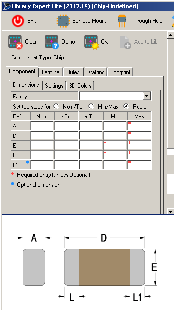
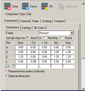
- Click the "Nom/Tol" radio button, enter the device dimensions,
four values from the Panasonic data sheet into the "Nom" column, for
rows A, D, E and L:
A = 0.60 = height (Z) of the resistor, from the t column of the data sheet.
D = 2.00 = length (X) of the resistor, from the L column.
E = 1.25 = width (Y) of the resistor, from the W column.
L = 0.40 = length (X) of the electrical contact, from the b column.
Then for those rows in the "- Tol" column, enter 0. In the "Family" pull-down list, select "Resistor". The result, for me, appeared as:
- Click the "OK" button. This will generate an updated
graphic display of the footprint, and seems to be necessary if we want
to change some items in other tabs and sub-tabs.
- This next step can be omitted - this is to show where we choose
the density level, which is how compact the software makes our
footprint. Click on the Terminal tab and then its Density Level sub-tab. The default is Nominal (N) which is what I want. The other options are Most and Least, and the actual values these presets control can be fine-tuned.
- This next step can be omitted - this is to show where we could
choose
the height and line-thickness of the silkscreen component legend text
and I think the lines on this layer which depict the outline of the
component. (I later decided to set the text size and line widths with
=a direct edit of the footprint file exported by Library Export Lite,
rather than relying on Library Expert Lite's settings - each of which
has to be manually set again for every fresh footprint which is
generated.) Click on the Drafting tab and then its Legend sub-tab. The defaults are presumably from IPC-7531: Outline Width from 0.12 to 0.10 and Ref. Des. Height from 1.20 to 1.00.
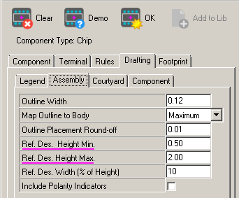
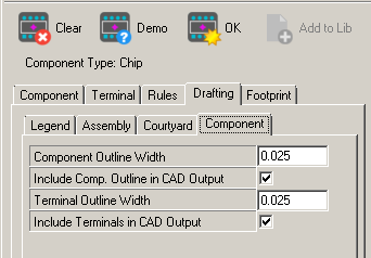
The sub-tab Assembly has similar settings for a rectangle which will be on KiCad's F.Fab layer, for an assembly drawing which shows the outline of the resistor.
The sub-tab Courtyard concerns a rectangle (or something more complex for larger, more complex-shaped components) which will be drawn on KiCad's F.CrtYd Courtyard layer, as well as an optional, default-on, cross-hair with circle ("target") at the X = 0, Y = 0 position (AKA the centroid). I didn't change anything. I am not sure that "Expand Courtyard to Include Legend" should be ticked, but it made no difference in this instance.
The sub-tab Component has settings for a set of thin lines which will be on KiCad's Dwgs.User layer. The lines create three rectangles in this example, one for the outline of the whole resistor and one each for each electrical terminal (contact).
Now select the Components tab again, with its Dimensions sub-tab, as depicted above.
- Click the "OK" button.
- If all is well, there will be no error message and the main
display window will show the footprint, with no grid or scale (but the
cursor can be used to show coordinates) and without some text items
which will appear in the exported KiCad footprint:
The pull-down list at the top left of this section of the window enables us to select something about the order the layers are drawn, but I don't yet understand it. The icon to its left, with four coloured bars, opens up a side-bar where we can choose the colours of the layers and whether they are on or off. See my cheatsheet0 image below. The above image results from the default layer on-and-off settings and with the default colours.
- Click the spanner icon at the right of the toolbar over the
display window. (If
you get an error such as one announcing an unhandled exception
regarding "Name
cannot begin with the '3' character, hexadecimal value 0x33. Line 3,
position 321." then this may be due to a line in a config file in the
program's installation directory, which for me: C:\Program Files
(x86)\PCB Libraries\Library Expert Lite 2017\FPXFormatPreferences.xml
. The program writes a keyword "3D_TOP" in the KiCad exporter
information, which it later objects to. This bug was fixed in the
release of 2017-19 available after about 2017-10-25, so you should be
able to avoid this by deleting the file or at least editing the keyword
to "THREED_TOP" and installing the bug-fixed version.)
- Select the "Translator" as "KiCad". I also selected "Set as Default Format".
- Select the output directory. Then the dialogue box should
look like this. The Top and Bottom layer names can be altered if
desired.
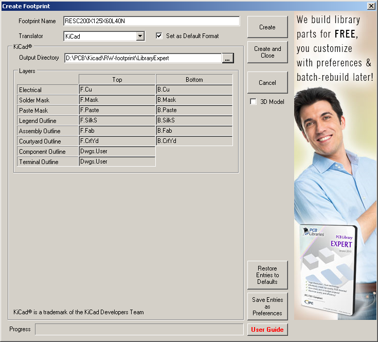
- Press the "Create" button. For me, this causes a file RESC200X125X60L40N.kicad_mod to be written to the output directory. This can be imported into Footprint Editor.
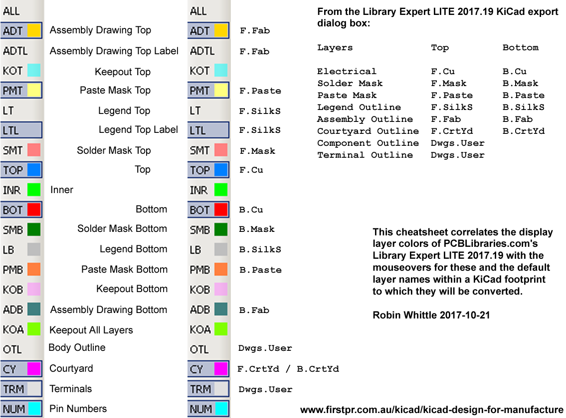
#cheatsheet0
Here is a cheatsheet correlating the default colours of Library Expert's layers, with their mouseover texts and the default layers they correspond to when the footprint is converted to a KiCad file. The full resolution version is: library-expert-layer-colours.png .
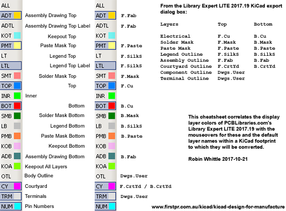
The last item NUM does not seem to be a layer, but enables the display of the pad numbers over the top of everything else. Right-clicking the colour box enables us to change the colour - except that some items such as ADTL do not have a colour, since this is set by the ADT item.
Three extra items appear (at least sometimes, for me) below item NUM:
Here are some examples of the display with only particular layers turned on:
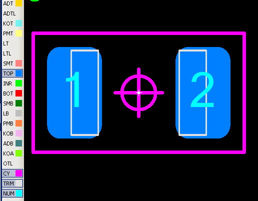
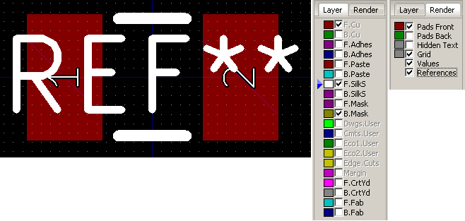
This shows the pads represented by Top copper (F.Cu) in blue, with pin numbers and the TRM layer showing the terminals. The magenta is Top Courtyard, which is converted to KiCad's F.CrtYd layer. The circle (target) and crosshairs can be turned off and resized in the various tab and sub-tabs mentioned above. The little white thing in the middle is not part of the footprint - this is Library Expert showing where 0,0 is.
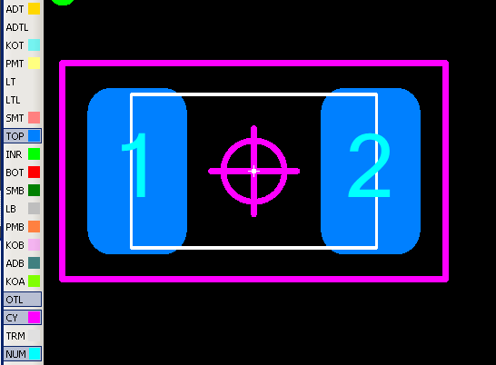
I turned off the terminals and turned on the Body Outline. Both these layers are converted to KiCad's Dwgs.User layer.
I understand the the Courtyard layer (there are front and back ones in KiCad) is used when laying out the PCB so that each component is kept a suitable distance from the other. I guess it may also be useful, with these crosshairs and targets, for the assembly company, but they should in principle be able to see where each component's centre is via the .POS file.

On top, because it was the most recent layer I turned on, is the Assembly Drawing Top's rectangle showing the outline of the resistor. The Assembly Drawing Top Label is depicted as well as Name, but all that matters to us is its orientation and position. This represents where two items will be in the converted footprint, both on the F.Fab layer, which is where the four lines of the rectangle will be as well: text value containing VAL** and text reference containing REF**. (See below for details of how KiCad interprets these fp_text items. From the exported footprint itself:
I was puzzled as to why the first item of text in the excerpt above is made so small: 0.77mm high. This is probably due to the fact that the whole component is small and the range of text sizes which are, by default in this program (presumably matching the specifications of the soon-to-be released IPC-7351C standard) set to 0.50mm to 2.00mm. This is in the Drafting tab > Assembly sub-tab:
Since my PCB fabricator http://www.pcbfast.com.au/techinfo/silkscreen-legends/ specifies for the silkscreen:
which preclude this part of the converted footprint from being used as is:
So the solution will be to alter these settings before creating components. This needs to be done for each component, as far as I know, with Library Expert Lite, but can be set in preference file for the Pro version.
#seeestudiodfm
Also, the widely-cited SeeedStudio document: http://www.seeedstudio.com/blog/2017/06/08/free-pcb-dfm-manual-v1-1-available-in-seeed-fusion/ states (page 7) that the silkscreen's minimum character height is 0.6mm and line width 0.1mm.
Once the footprint is placed in the PCB design, we can change these things manually, but it would probably be best to get the footprint in the library set so its default state doesn't violate the restrictions on what we can have made. These changes can be made in Footprint Editor, but it might be better to tweak Library Expert Lite to set the values within proper limits. (Later I decided to set the size of these text items on all layers to 0.8mm in a later edit of the footprint file, before importing it into Footprint Editor for review and saving to my library.)
There are three separate layers in this Library Expert system (for the top = front side) which correspond to the pad:
however they all show the same thing, in this example, and at least for this particular footprint, all three aspects of the pad are defined in a single line for each pad, all with the same size:
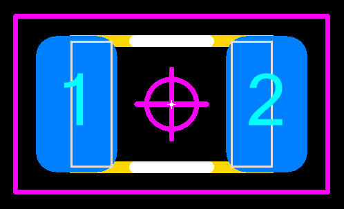
Here is the image which results from the final combination of layers turned on:

The two lines are the silkscreen indication of the location of the resistor. Other footprints have more elaborate arrangements, including the presence or absence of a line within this shape to indicate polarity (the location of pin 1, or the positive terminal etc.) - or alternatively the presence of a dot to indicate this. IPC-7351C specifies that no part of the silkscreen image should be in the same place, or close to, a pad, or be covered up by the component once it is assembled. However, at the level of the footprint library, it makes sense to have the initial location of the reference text in the centre of the footprint, to make things easier when we are moving them around to their final locations in the PCB layout, before laying tracks and moving the text items to their final locations.
In both Pcbnew and Footprint Editor (this is with a Windows nightly from 2017-09-19) I changed some layer colours:
F.SilkS White
Dwgs.User Green 4
F.CrtYd Magenta 4
F.Fab Cyan 3
Once imported into Footprint Editor, this footprint's initial appearance is:

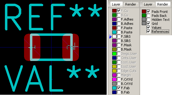
Here is the F.cu , F.CrtYd and Dwgs.User , with Hidden Text, Values and References not displayed:
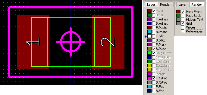
The resistor outline and terminal rectangles are superimposed on the Dwgs.User layer, but they are all separate lines so I could alter them if I wished, such as to show only the component outline. Alternatively I could have set Library Expert Lite to show only the outline and not the terminals by altering some settings in the Drafting tab > Assembly sub-tab from what I used, by default:
Next, we see just the pads and the silkscreen, with Values and References displayed.
I edited the pads to be rounded rectangles, by right clicking pad 1 and selecting Rounded Rectangle, and then by right clicking pad 2 and selecting Apply Pad Settings, which requires no further action to make the same change to the second pad. I turned off the F.Silk layer and turned on F.Fab and moved the REF** text up and the VAL** text down, to reduce clutter. However, this would not be a change I make to the footprint - best to keep them in the central location to simplify moving the instances of footprints around the PCB design in the early stages of the design. Also, it is possible to turn on and off the display of References and Values, in Footprint Editor and in Pcbnew, which means they can be in the centre of the component and not clutter each other up if we use these display options selectively:
#roundedrectangles
Here is the text of the footprint, as exported from Footprint Editor, after a single change: selecting rounded rectangle pads. The order but not the content of the first and third fp_text items has been reversed by this process. The only other changes are in red: a timestamp and the extra text for rounded rectangles:
So far, so good. I have created an apparently IPC-7351C-compliant
footprint, based on looking up a manufacturer's datasheet to get the
physical dimensions of the component, and I have exported it into KiCad
and changed the pads to rounded rectangles.
But is this really what I want? How would I know? I haven't yet designed a proper PCB with KiCad, much less had the boards made and automatically assembled.
So I contemplated this simple footprint in the light of what I could glean from far more experienced people who wrote in thread00. They were writing in mid-2016, when KiCad's capabilities were perhaps somewhat different.
For me, the most significant material in this thread was written by Mars_Warrior, including these two messages: https://forum.kicad.info/t/why-are-the-kicad-library-conventions-non-ipc-compliant/3678/12 and https://forum.kicad.info/t/why-are-the-kicad-library-conventions-non-ipc-compliant/3678/62 .
"fabhouse" means the company which does automated SMT assembly. (I use the term "PCB fabricator" to refer to the company which makes the bare printed circuit boards.) "refdes" means the reference, or reference designator, for instance U4, C37 etc.
Here is a cheatsheet correlating the default colours of Library Expert's layers, with their mouseover texts and the default layers they correspond to when the footprint is converted to a KiCad file. The full resolution version is: library-expert-layer-colours.png .
The last item NUM does not seem to be a layer, but enables the display of the pad numbers over the top of everything else. Right-clicking the colour box enables us to change the colour - except that some items such as ADTL do not have a colour, since this is set by the ADT item.
Three extra items appear (at least sometimes, for me) below item NUM:
- GRID Right click to set the X and Y dimensions, but I don't see any grid.
- BG Background colour.
- HLT
Highlight colour. The cursor, together with potentially the
control key can be used to select one or more things, but I could only
get it to work with pads at first, until I discovered that by right
clicking in an empty area of the display window, I can select which of Pins, Shapes, Lines and Labels are available for selection. Once an item is selected, right-click
brings up a properties box.
Here are some examples of the display with only particular layers turned on:
This shows the pads represented by Top copper (F.Cu) in blue, with pin numbers and the TRM layer showing the terminals. The magenta is Top Courtyard, which is converted to KiCad's F.CrtYd layer. The circle (target) and crosshairs can be turned off and resized in the various tab and sub-tabs mentioned above. The little white thing in the middle is not part of the footprint - this is Library Expert showing where 0,0 is.
I turned off the terminals and turned on the Body Outline. Both these layers are converted to KiCad's Dwgs.User layer.
I understand the the Courtyard layer (there are front and back ones in KiCad) is used when laying out the PCB so that each component is kept a suitable distance from the other. I guess it may also be useful, with these crosshairs and targets, for the assembly company, but they should in principle be able to see where each component's centre is via the .POS file.
On top, because it was the most recent layer I turned on, is the Assembly Drawing Top's rectangle showing the outline of the resistor. The Assembly Drawing Top Label is depicted as well as Name, but all that matters to us is its orientation and position. This represents where two items will be in the converted footprint, both on the F.Fab layer, which is where the four lines of the rectangle will be as well: text value containing VAL** and text reference containing REF**. (See below for details of how KiCad interprets these fp_text items. From the exported footprint itself:
(fp_text user %R (at 0 0) (layer F.SilkS)
(effects (font (size 0.77 0.77) (thickness 0.08)))
)
(fp_text value VAL** (at 0 0) (layer F.Fab)
(effects (font (size 1.2 1.2) (thickness 0.12)))
)
(fp_text reference REF** (at 0 0) (layer F.Fab)
(effects (font (size 1.2 1.2) (thickness 0.12)))
)
(effects (font (size 0.77 0.77) (thickness 0.08)))
)
(fp_text value VAL** (at 0 0) (layer F.Fab)
(effects (font (size 1.2 1.2) (thickness 0.12)))
)
(fp_text reference REF** (at 0 0) (layer F.Fab)
(effects (font (size 1.2 1.2) (thickness 0.12)))
)
I was puzzled as to why the first item of text in the excerpt above is made so small: 0.77mm high. This is probably due to the fact that the whole component is small and the range of text sizes which are, by default in this program (presumably matching the specifications of the soon-to-be released IPC-7351C standard) set to 0.50mm to 2.00mm. This is in the Drafting tab > Assembly sub-tab:
Since my PCB fabricator http://www.pcbfast.com.au/techinfo/silkscreen-legends/ specifies for the silkscreen:
Inkjet Liquid Photo Imaging (More expensive.)
Min text height 0.80mm 0.50mm
Min line width 0.15mm 0.10mm
Min text height 0.80mm 0.50mm
Min line width 0.15mm 0.10mm
which preclude this part of the converted footprint from being used as is:
(effects (font (size 0.77 0.77) (thickness 0.08)))
So the solution will be to alter these settings before creating components. This needs to be done for each component, as far as I know, with Library Expert Lite, but can be set in preference file for the Pro version.
#seeestudiodfm
Also, the widely-cited SeeedStudio document: http://www.seeedstudio.com/blog/2017/06/08/free-pcb-dfm-manual-v1-1-available-in-seeed-fusion/ states (page 7) that the silkscreen's minimum character height is 0.6mm and line width 0.1mm.
Once the footprint is placed in the PCB design, we can change these things manually, but it would probably be best to get the footprint in the library set so its default state doesn't violate the restrictions on what we can have made. These changes can be made in Footprint Editor, but it might be better to tweak Library Expert Lite to set the values within proper limits. (Later I decided to set the size of these text items on all layers to 0.8mm in a later edit of the footprint file, before importing it into Footprint Editor for review and saving to my library.)
There are three separate layers in this Library Expert system (for the top = front side) which correspond to the pad:
PMT Paste Mask Top
SMT Solder Mask Top
TOP Top (copper)
SMT Solder Mask Top
TOP Top (copper)
however they all show the same thing, in this example, and at least for this particular footprint, all three aspects of the pad are defined in a single line for each pad, all with the same size:
(pad 1 smd rect (at -0.95 0) (size 0.81 1.36) (layers F.Cu F.Paste F.Mask))
(pad 2 smd rect (at 0.95 0) (size 0.81 1.36) (layers F.Cu F.Paste F.Mask))
(pad 2 smd rect (at 0.95 0) (size 0.81 1.36) (layers F.Cu F.Paste F.Mask))
Here is the image which results from the final combination of layers turned on:
The two lines are the silkscreen indication of the location of the resistor. Other footprints have more elaborate arrangements, including the presence or absence of a line within this shape to indicate polarity (the location of pin 1, or the positive terminal etc.) - or alternatively the presence of a dot to indicate this. IPC-7351C specifies that no part of the silkscreen image should be in the same place, or close to, a pad, or be covered up by the component once it is assembled. However, at the level of the footprint library, it makes sense to have the initial location of the reference text in the centre of the footprint, to make things easier when we are moving them around to their final locations in the PCB layout, before laying tracks and moving the text items to their final locations.
In both Pcbnew and Footprint Editor (this is with a Windows nightly from 2017-09-19) I changed some layer colours:
F.SilkS White
Dwgs.User Green 4
F.CrtYd Magenta 4
F.Fab Cyan 3
Once imported into Footprint Editor, this footprint's initial appearance is:
Here is the F.cu , F.CrtYd and Dwgs.User , with Hidden Text, Values and References not displayed:
The resistor outline and terminal rectangles are superimposed on the Dwgs.User layer, but they are all separate lines so I could alter them if I wished, such as to show only the component outline. Alternatively I could have set Library Expert Lite to show only the outline and not the terminals by altering some settings in the Drafting tab > Assembly sub-tab from what I used, by default:
Next, we see just the pads and the silkscreen, with Values and References displayed.
I edited the pads to be rounded rectangles, by right clicking pad 1 and selecting Rounded Rectangle, and then by right clicking pad 2 and selecting Apply Pad Settings, which requires no further action to make the same change to the second pad. I turned off the F.Silk layer and turned on F.Fab and moved the REF** text up and the VAL** text down, to reduce clutter. However, this would not be a change I make to the footprint - best to keep them in the central location to simplify moving the instances of footprints around the PCB design in the early stages of the design. Also, it is possible to turn on and off the display of References and Values, in Footprint Editor and in Pcbnew, which means they can be in the centre of the component and not clutter each other up if we use these display options selectively:
#roundedrectangles
Here is the text of the footprint, as exported from Footprint Editor, after a single change: selecting rounded rectangle pads. The order but not the content of the first and third fp_text items has been reversed by this process. The only other changes are in red: a timestamp and the extra text for rounded rectangles:
(module RESC200X125X60L40N (layer F.Cu) (tedit 59EB4182) (descr "Resistor, Chip; 2.00 mm L X 1.25 mm W X 0.60 mm H body") (attr smd) (fp_text reference REF** (at 0 0) (layer F.Fab) (effects (font (size 1.2 1.2) (thickness 0.12))) )
(fp_text value VAL** (at 0 0) (layer F.Fab)
(effects (font (size 1.2 1.2) (thickness 0.12)))
)
(fp_text user %R (at 0 0) (layer F.SilkS)
(effects (font (size 0.77 0.77) (thickness 0.08)))
)
(fp_line (start -0.6 -0.625) (end -0.6 0.625) (layer Dwgs.User) (width 0.025))
(fp_line (start -0.6 0.625) (end -1 0.625) (layer Dwgs.User) (width 0.025))
(fp_line (start -1 0.625) (end -1 -0.625) (layer Dwgs.User) (width 0.025))
(fp_line (start -1 -0.625) (end -0.6 -0.625) (layer Dwgs.User) (width 0.025))
(fp_line (start 0.6 0.625) (end 0.6 -0.625) (layer Dwgs.User) (width 0.025))
(fp_line (start 0.6 -0.625) (end 1 -0.625) (layer Dwgs.User) (width 0.025))
(fp_line (start 1 -0.625) (end 1 0.625) (layer Dwgs.User) (width 0.025))
(fp_line (start 1 0.625) (end 0.6 0.625) (layer Dwgs.User) (width 0.025))
(fp_line (start -1 0.625) (end -1 -0.625) (layer Dwgs.User) (width 0.025))
(fp_line (start -1 -0.625) (end 1 -0.625) (layer Dwgs.User) (width 0.025))
(fp_line (start 1 -0.625) (end 1 0.625) (layer Dwgs.User) (width 0.025))
(fp_line (start 1 0.625) (end -1 0.625) (layer Dwgs.User) (width 0.025))
(fp_line (start -1 0.63) (end -1 -0.63) (layer F.Fab) (width 0.12))
(fp_line (start -1 -0.63) (end 1 -0.63) (layer F.Fab) (width 0.12))
(fp_line (start 1 -0.63) (end 1 0.63) (layer F.Fab) (width 0.12))
(fp_line (start 1 0.63) (end -1 0.63) (layer F.Fab) (width 0.12))
(fp_line (start -0.365 -0.63) (end 0.365 -0.63) (layer F.SilkS) (width 0.12))
(fp_line (start -0.365 0.63) (end 0.365 0.63) (layer F.SilkS) (width 0.12))
(fp_line (start -1.56 0.88) (end -1.56 -0.88) (layer F.CrtYd) (width 0.05))
(fp_line (start -1.56 -0.88) (end 1.56 -0.88) (layer F.CrtYd) (width 0.05))
(fp_line (start 1.56 -0.88) (end 1.56 0.88) (layer F.CrtYd) (width 0.05))
(fp_line (start 1.56 0.88) (end -1.56 0.88) (layer F.CrtYd) (width 0.05))
(fp_circle (center 0 0) (end 0 0.25) (layer F.CrtYd) (width 0.05))
(fp_line (start 0.35 0) (end -0.35 0) (layer F.CrtYd) (width 0.05))
(fp_line (start 0 -0.35) (end 0 0.35) (layer F.CrtYd) (width 0.05))
(pad 1 smd roundrect (at -0.95 0) (size 0.81 1.36) (layers F.Cu F.Paste F.Mask)(roundrect_rratio 0.25))
(pad 2 smd roundrect (at 0.95 0) (size 0.81 1.36) (layers F.Cu F.Paste F.Mask)(roundrect_rratio 0.25))
)
But is this really what I want? How would I know? I haven't yet designed a proper PCB with KiCad, much less had the boards made and automatically assembled.
So I contemplated this simple footprint in the light of what I could glean from far more experienced people who wrote in thread00. They were writing in mid-2016, when KiCad's capabilities were perhaps somewhat different.
For me, the most significant material in this thread was written by Mars_Warrior, including these two messages: https://forum.kicad.info/t/why-are-the-kicad-library-conventions-non-ipc-compliant/3678/12 and https://forum.kicad.info/t/why-are-the-kicad-library-conventions-non-ipc-compliant/3678/62 .
"fabhouse" means the company which does automated SMT assembly. (I use the term "PCB fabricator" to refer to the company which makes the bare printed circuit boards.) "refdes" means the reference, or reference designator, for instance U4, C37 etc.
davidsrsb:
In August 2016 the then current Library Expert Lite apparently did most
of what Mars_Warrior wanted, including long, detailed,
all-metric, IPC-7351C compliant names for footprints (SOIC14P127_865X600X172L84X41N.kicad_mod) and the Level B zero rotation orientation, which I discuss further below.
He made changes to the Library Expert Lite footprints to achieve the
2 changes
which he needed in addition, which are, according to my
understanding, and thinking only of the front (top) side of the PCB
(and here I am referring to the footprint files exported by the 2017-19
version of Library Expert Lite, not whatever potentially different
format Mars_Warrior was working with from earlier versions of this
program):I would have thought the place to put value is on a fabrication layer in the component courtyard. The value is there for the assembler or QA inspector
Mars_Warrior:
No, the reference is used by the fabhouse to know which component is placed where. Apart from the value, there are more specifications for a component that are needed than the value, eg. manufacturer, power etc. This is with the refdes listed in the BOM.
My silkscreens just show the refdes. I use a separate layer in Kicad (eco1.user) to show the value of each component. There is just no place for a value on a PCB with lots of SMD components.
F.Fab Outline
of component (this is already there in the Library Expert Lite
footprint) with the RefDes ("reference" AKA "reference designator")
text displayed, as a result the fp_text item of type reference for F.Fab.
Change 1 involves altering the layer of the fp_text item of type value from F.Fab to Eco1.User.
Change 2 involves copying the lines specifying whatever graphic elements are currently assigned to the F.Fab layer, and altering the copies so they are assigned to the Eco1.User layer.
Change 1 involves altering the layer of the fp_text item of type value from F.Fab to Eco1.User.
Change 2 involves copying the lines specifying whatever graphic elements are currently assigned to the F.Fab layer, and altering the copies so they are assigned to the Eco1.User layer.
There is an example below of these change. These changes are not the same as what changes I would make to a footprint file which followed the KiCad Library Conventions (see below), since such a file is somewhat different from the file generated by Library Expert Lite.
I understand that Mars_Warrior wants the F.Fab layer to produce a drawing which a PCB assembly company can use, so that every SMT component they are going to mount has an outline and the RefDes (reference) text. From this, they can look up all the details, such as part number, value (e.g. uF and voltage, or resistance, or a range of possible part numbers, each with links to suppliers websites) in the BoM file.
I understand he wants the Eco1.User layer to produce a similar drawing, for when he is hand-assembling a board. This has the same component outlines, but has the value instead - such as a simple resistance (2K7), capacitance (334), connector part number, microcontroller part number etc. - so he can instantly see what to place in each location. I think this is primarily for SMT components which are so small and densely packed that it may not be possible to have any text for many of them on the board itself (F.SilkS) and it would generally be impossible to have values on F.SilkS in addition to the reference text, even if there was room for the reference text.
It doesn't matter much how small the text is for reference and value on the F.Fab or Eco1.User layers since these are not part of the physical circuit board. It is easy to zoom on on these when looking at the computer monitor, or print these layers on large enough pieces of paper that the text can be read. With the silkscreen layer, the text really needs to be outside the body and pins of the component, whereas this is not a restriction on F.Fab, Eco1.User or other non-physical layers. So it is possible and desirable on the F.Fab and Eco1.User layers to have the outline of the component and the text of either the reference or the value, potentially inside the outline. In principle it might be possible and desirable to have both the reference (C12 etc.) and the value (104 etc.) on the same layer, but that could be cluttered and the part numbers or values can be very long.
According to the Pcbnew manual (2017-08-24 version), page 37:
Edge.Cuts
is reserved for the drawing of circuit board outline. Any element
(graphic, texts…) placed on this layer appears on all the other layers.
Use this layer only to draw board outlines.
This duplication of text does not suit my needs for a layer to send to PCBFast.com.au, which has lines to describe routed (milled) edges and text regarding this and perhaps other things. In principle I could choose to put this information on Dwgs.User, but that is already in use with the outlines of the components and their terminals (at least for the above example).
On this page, the purpose of the Fabrication layers is not clearly defined:
Fabrication (F.Fab and B.Fab) Footprint assembly (?).
Following Mars Warrior's example I will use Eco1.User as he does, which leaves Eco2.User for my routing (milling) and other mechanical information, which is needed by the PCB fabricator.
The way I (and I think Mars Warrior and Joan Sparky, both of whom post to the KiCad forum) want to use KiCad appears to be different from the usage pattern supported by the KiCad library standard, formally known as the KiCad Library Convention, hereafter KLC (I am referring to rev 3.0.0 on 2017-11-03):
Until early November 2017, the KLC (rev 2.0.12) was here:
Section F5.2 (2017-11-04) requires that footprints in the footprint library that the F.Fab layer have three things for each footprint:
1 - The component outline.
2 - The value text: "Component value (footprint name)".
3 - The reference text, by way of a %R construct: "Reference Designator . . . Centered on component (inside component outline) . . .".
2 - The value text: "Component value (footprint name)".
3 - The reference text, by way of a %R construct: "Reference Designator . . . Centered on component (inside component outline) . . .".
Section F5.1 (2017-11-04) requires that footprints in the footprint library that the F.SilkS layer has only one text item things for each footprint:
1 - The reference text.
2 - Pin 1 designator where appropriate, according to IPC-7351C.
3 - Component outlines and other graphic elements (my paraphrase of the detailed specifications) which should be visible, along with the reference text and pin 1 designator, after the component is mounted, plus, for through hole components only, some optional presumably graphic elements: "Silkscreen may be placed under component to aid in assembly".
Now it is time to consider the mechanism of fp_text items in footprints, in the footprint library and for footprints in a PCB design within Pcbnew, as they are automatically placed, then then manually edited. This is quite tricky since I am considering several steps:
1 - Generating an initial footprint
file from Library Expert, from some other generator, or by copying a
footprint from some library, including the standard KiCad library.
2 - Editing it manually (in the future I might write a program to do some or all of this) to get it into the state I want for:
3 - Importing the edited footprint file into Footprint Editor.
4 - Viewing and checking the results of the import and potentially making other changes in Footprint Editor.
5 - Saving the results to the current library.
I am also thinking about how the footprint behaves when Pcbnew loads it from my footprint library (I currently have only one) into a PCB design due to manual placement, automatic placement due to loading a netlist - and how it behaves if the footprint is already in the PCB design but is somehow updated as a result of a netlist load. (To do: when does this occur???)
My primary interest is what state the footprint file must be in before being imported into Footprint Editor. What follows is based on my understanding of the program (Windows nightlies 2017-09-19 and 2019-11-01), various forum discussions and some source code :
https://github.com/KiCad/kicad-source-mirror/blob/master/pcbnew/class_text_mod.h
https://github.com/KiCad/kicad-source-mirror/blob/master/pcbnew/class_text_mod.cpp
https://github.com/KiCad/kicad-source-mirror/blob/master/pcbnew/class_text_mod.cpp
Text items in the footprint file which is ready to be imported into Footprint Editor
The slightly edited version above #roundedrectangles of a footprint exported from Library Expert Lite contains three fp_text items ("item" is my term): (fp_text reference REF** (at 0 0) (layer F.Fab)
(effects (font (size 1.2 1.2) (thickness 0.12)))
)
(fp_text value VAL** (at 0 0) (layer F.Fab)
(effects (font (size 1.2 1.2) (thickness 0.12)))
)
(fp_text user %R (at 0 0) (layer F.SilkS)
(effects (font (size 0.77 0.77) (thickness 0.08)))
)
All three contain specifications for the location of the text relative to the centre of the footprint "(at 0 0)", for the height and width of the characters and for the line
thickness with which they will be drawn. All three have a section
specifying which layer the text item's final text will appear on.
This is for visual display in Pcbnew and for output via printing,
plotting and SVG export.Here is another perfectly valid text item:
(fp_text user "ABC %R XYZ %V POQ" (at 0 0) (layer F.SilkS)
(effects (font (size 0.77 0.77) (thickness 0.08)))
)Once such a footprint with such an fp_text item has been placed on the PCB design, with reference C2 and value 104, the F.SilkS layer will display:ABC C2 XYZ 104 POQ
There are three types of fp_text item:
| Word which follows fp_text and the matching TEXT_TYPE enumeration from the above-mentioned header file. |
How
many items of this type will be recognised when the file is imported
into Footprint Editor and the results are saved to the current library? |
Does the text following the type word (reference, value or user)
arrive in the instance of the footprint which is part of a PCB design
after being placed due to loading a netlist? (These are
displayed verbatim within Footprint Editor.) What about when manually placing a footprint, which does not, at first, involve assigning a proper reference or value to it? |
| reference TEXT_is_REFERENCE |
One. It
seems that the last one of two or more such items is used and any prior
text item is ignored unless it is the only value text item. The saved footprint file has the reference text item first, before the value text item. To keep things simple, the file I import into Footprint Editor should have this reference text item first - and it should follow the (descr . . .) item. |
No. Whatever text was there is ignored, and the reference of this instance of the footprint is displayed. Subsequent changes to the reference of this instance of the footprint, via the "Footprint Properties" dialogue box ("E" or right-click > Edit Footprint Parameters) > Properties tab > Reference > Edit (creates a new dialogue box "Footprint Text Properties"), will change the text which is visible for fp_text item. This "Footprint Text Properties" dialogue box can also change the layer on which this fp_text item appears and other details such as size, character line thickness and rotation etc. The same changes with the same type of "Footprint Text Properties"dialogue box can be made by editing the text as it appears on a given layer, for instance by editing directly the text on the particular layer, which may appear for instance as C123 initially. Changing that to C456 changes the reference of the footprint. Whatever text followed fp_text reference in the footprint file in the library is used as the reference for the newly placed footprint. This is generally inconsequential, firstly because KiCad usage doesn't usually involve manual placement - generally every footprint on the PCB should be there because it is mentioned in the netlist - and since if the user does manually place a footprint, he or she will soon edit it to have the desired reference. |
| value TEXT_is_VALUE |
One, presumably with similar behaviour to that mentioned above. To keep things simple, the file I import into Footprint Editor should have this value text item second. |
As above, except that this is for the value of the footprint in the PCB design. |
| user TEXT_is_DIVERS |
Zero or more. In the file I import into Footprint Editor, any such text items should follow both the reference and value text items and precede all the graphic elements and pads. | This text can be whatever is desired, with the special provision that if one of these two constructs are used: %R or %V
the component's (that is: of the instance of this footprint in the PCB design which we think of as a component) reference text or value text will be displayed in place of
each construct. So it is possible to precede and follow the text
of the reference or value with arbitrary text, and these constructs can
be used any number of times within a particular fp_text item. If the total text contains one or more spaces, then it should be in double quotes. For instance if the footprint in the PCB design has a value of 100uF and there is a user fp_text item for F.SilkS: (fp_text user %V (at 0 . . . then 100uF will appear on the F.SilkS layer. Changing the value of the footprint, by editing the footprint itself, will cause the new value to be displayed. Editing the text as it appears on the the F.SilkS layer will result in a "Footprint Text Properties" dialogue box as mentioned above, but the text to be edited will NOT be 100uF or whatever the value of this footprint is currently set to, it will be %V. This can be changed arbitrarily. |
which states, regarding the reference and value types of fp_text item:
The
type field can be "reference", "value" or "user". For a library the
text for the reference and value are place-holders; they will be
replaced by the actual reference and value texts.
From this, I observe:
- We can use %R and %V
as we desire in fp_text items of type user to display the reference and
value of this instance of the footprint in a PCB (this component in a
PCB).
- A particular instance of a footprint in a PCB design (a particular component) has a reference, and a single fp_text item of type reference
which causes this reference text to be displayed on a particular
layer. Editing the text on that layer (as opposed to formally
changing the reference in the Footprint Properties dialogue box) DOES
change the reference.
So the fp_text item of type reference creates a visible and editable piece of text on exactly one layer. That layer can be changed. That text on that layer always appears as whatever the reference text of the footprint is, and editing that layer's text changes the reference.
The KLC specifies that this fp_text item of type reference be for the F.SilkS layer. As far as I know, in KiCad library footprints, the text given for this item is usually REF** - but this is just an arbitrary placeholder to provide something for Footprint Editor to display. (It is also used as the reference text for the instance of a footprint which has been manually placed, but manual placement of footprints is not a normal part of the KiCad approach to PCB design.)
I think this KLC specification is compatible with my approach. For this to be the case, I would have to accept that if there was to be any text printed on the PCB via the F.SilkS layer directly as part of the instance of this footprint on the PCB (this component) then that text will be precisely the reference of this instance.
I can always hide this and add a separate text item if I want something else to appear instead, but this will not be part of the instance - it will just be some text I place manually in the PCB design on the F.SilkS layer. This should be fine.
- Likewise, each instance of a footprint in a PCB design has a value, which is directly linked to a single fp_text item of type value which causes this value text to be displayed on a particular layer.
The KLC specifies that this fp_text item of type value be for the F.Fab layer. As far as I know, in KiCad library footprints, the text given for this item is usually the same as the footprint name - but this is just an arbitrary placeholder to provide something for Footprint Editor to display and to be the value of a newly manually placed instance of a footprint in a PCB design.
This KLC specification is NOT compatible with my approach.
I don't want the value on the F.Fab layer - I want the reference, so I create a separate fp_text item of type user for the F.Fab layer, and set its text to %R. (Change A.)
I want the value to be on the Eco1.User layer, and since this is the only layer on which the value will appear, I will change the fp_text item of type value so it is for the Eco1.User layer instead of the F.Fab layer. (Change B.) Therefore, if I edit this text on the Eco1.User layer, it will change the value of this instance of the footprint.
I also make a copy of the component outline graphics of F.Fab to Eco1.User. (Change C.)
Broadly speaking, there are three types of footprint file I am considering:
- Those which adhere to the KLC rules.
- Those which are produced by Library Expert Lite.
- Modified versions of both kinds of files which suit my purposes
and are ready to be imported into Footprint Editor, for visual review
and possible further changes, before storing the results in the current
library.
The 2017-19 version of Library Expert Lite does not produce anything for the Eco1.User layer. As I understand its options, the component outline, fp_text reference and fp_text value for the top of the PCB are all put on whatever KiCad layer we like - and F.Fab is the default - by way of the "Assembly Outline" line in the KiCad exporter options.
My understanding (late October 2017 with Library Expert Lite 2017-19 and a KiCad nightly from 2017-09-19) is:
Library Expert Lite does not actually display both the REF** and VAL**
texts (these are created by its KiCad exporter), but can turn on and off the display of the word "Name" via the
Manage Layer Display bar (click the blue-orange-orange-red banded
button) ADTL button (Assembly Drawing Top Label). However, this is not the important question.
When an unmodified footprint file from Library Expert Lite is imported into Footprint editor, saved into a library and the resulting footprint in the library is used to place an instance of this footprint (a component) into a PCB design, Pcbnew displays the component's reference (due to the fp_text reference) and the value (due to the fp_text value) texts when the F.Fab layer is displayed, and the display of each is specifically controlled by the Visibles > Render > Values and Reference check boxes.
If Pcbnew's Print, SVG Export and Plot facilities provided a similar ability to individually control the printing of references and values, then I think Mars_Warrior's aim (and mine) could be achieved without any changes to the footprint file exported by Library Expert Lite. However, no such controls exist, so we need to modify the footprint file before importing it into Footprint Editor.
I want these same capabilities that Mars_Warrior wants. I am using the Eco2.User
layer for text and lines to show the edges of the individual final
PCBs, which will be routed with a 2mm router bit. The text may
also be used for other mechanical instructions for the PCB manufacturer,
as requested here:
The third page states that they use CAM350 software for working with Gerber and drill files, and this page: http://www.downstreamtech.com/cam350.php states that CAM350 is the industry standard software for PCB fabricators, and that it generates final Gerber files, final drill files and instructions for routing (milling) machines.
I can achieve it by editing the footprint file exported by Library Expert Lite in the following ways (this is not counting the changes required to implement rounded rectangle pads):
Here is the footprint, as produced by Library Expert Lite, with these changes in blue for new text and red for that which has been deleted with each change labeled. The violet change is due to me changing the footprint's name here, and in its filename, to become RESC200X125X60L40N-2012i0805 as I describe in a section below: #footprintnames. The changes in pale aqua are the same as those mentioned above #roundedrectangles for the additional changes which could be made manually, or with Footprint Editor, to make the pads rounded rectangles. F.Fab is highlighted in black.
This is relatively simple to do manually for small numbers of footprints. Alternatively, I could write a program to
do it. It would also make sense for such a program to make the
rounded rectangle changes too. So the program would process the
just-exported footprint to create a modified file which would be
manually imported into Footprint Editor, checked, perhaps edited some
more, and then saved in my library.
Since I also want to change some of the text sizes from those in the footprint as exported by Library Expert Lite, rather than editing the lines as shown above, much of what I need - Changes 1, 2 and 3 - can be achieved simply by pasting a standard block of text for all my footprints to implement the three fp_text items. The block to past in is:
#blocktopaste
http://www.pcbfast.com.au/techinfo/rout/
http://www.pcbfast.com.au/techinfo/accepted-data/gerber-274x/
http://www.pcbfast.com.au/techinfo/multi-design-panels/
http://www.pcbfast.com.au/techinfo/accepted-data/gerber-274x/
http://www.pcbfast.com.au/techinfo/multi-design-panels/
The third page states that they use CAM350 software for working with Gerber and drill files, and this page: http://www.downstreamtech.com/cam350.php states that CAM350 is the industry standard software for PCB fabricators, and that it generates final Gerber files, final drill files and instructions for routing (milling) machines.
I can achieve it by editing the footprint file exported by Library Expert Lite in the following ways (this is not counting the changes required to implement rounded rectangle pads):
| Change the layer of the fp_text user %R item from F.SilkS to F.Fab. | Change 1. |
| Change the layer of the fp_text reference item from F.Fab to F.SilkS. | Change 2. |
| Change the layer of the fp_text value item from F.Fab to Eco1.User. | Change 3 = Change B above for KLC-style footprints. |
| Make a copy of the component outline graphics of F.Fab to Eco1.User. |
Change 4 = Change C above for KLC-style footprints. |
Here is the footprint, as produced by Library Expert Lite, with these changes in blue for new text and red for that which has been deleted with each change labeled. The violet change is due to me changing the footprint's name here, and in its filename, to become RESC200X125X60L40N-2012i0805 as I describe in a section below: #footprintnames. The changes in pale aqua are the same as those mentioned above #roundedrectangles for the additional changes which could be made manually, or with Footprint Editor, to make the pads rounded rectangles. F.Fab is highlighted in black.
(module RESC200X125X60L40N-2012i0805 (layer F.Cu) (tedit 0)
  (descr "Resistor, Chip; 2.00 mm L X 1.25 mm W X 0.60 mm H body")
  (attr smd)
  (fp_text user %R (at 0 0) (layer F.SilkSF.Fab)                                   Change 1
    (effects (font (size 0.77 0.77) (thickness 0.08)))
  )
  (fp_text value VAL** (at 0 0) (layer F.FabEco1.User)                             Change 3
    (effects (font (size 1.2 1.2) (thickness 0.12)))
  )
  (fp_text reference REF** (at 0 0) (layer F.FabF.SilkS)                           Change 2
    (effects (font (size 1.2 1.2) (thickness 0.12)))
  )
  (fp_line (start -0.6 -0.625) (end -0.6 0.625) (layer Dwgs.User) (width 0.025))
  (fp_line (start -0.6 0.625) (end -1 0.625) (layer Dwgs.User) (width 0.025))
  (fp_line (start -1 0.625) (end -1 -0.625) (layer Dwgs.User) (width 0.025))
  (fp_line (start -1 -0.625) (end -0.6 -0.625) (layer Dwgs.User) (width 0.025))
  (fp_line (start 0.6 0.625) (end 0.6 -0.625) (layer Dwgs.User) (width 0.025))
  (fp_line (start 0.6 -0.625) (end 1 -0.625) (layer Dwgs.User) (width 0.025))
  (fp_line (start 1 -0.625) (end 1 0.625) (layer Dwgs.User) (width 0.025))
  (fp_line (start 1 0.625) (end 0.6 0.625) (layer Dwgs.User) (width 0.025))
  (fp_line (start -1 0.625) (end -1 -0.625) (layer Dwgs.User) (width 0.025))
  (fp_line (start -1 -0.625) (end 1 -0.625) (layer Dwgs.User) (width 0.025))
  (fp_line (start 1 -0.625) (end 1 0.625) (layer Dwgs.User) (width 0.025))
  (fp_line (start 1 0.625) (end -1 0.625) (layer Dwgs.User) (width 0.025))
  (fp_line (start -1 0.63) (end -1 -0.63) (layer F.Fab) (width 0.12))
  (fp_line (start -1 -0.63) (end 1 -0.63) (layer F.Fab) (width 0.12))
  (fp_line (start 1 -0.63) (end 1 0.63) (layer F.Fab) (width 0.12))
  (fp_line (start 1 0.63) (end -1 0.63) (layer F.Fab) (width 0.12))
  (fp_line (start -1 0.63) (end -1 -0.63) (layer Eco1.User) (width 0.12))         } Change 4
  (fp_line (start -1 -0.63) (end 1 -0.63) (layer Eco1.User) (width 0.12))         }
  (fp_line (start 1 -0.63) (end 1 0.63) (layer Eco1.User) (width 0.12))           }
  (fp_line (start 1 0.63) (end -1 0.63) (layer Eco1.User) (width 0.12))	          }
  (fp_line (start -0.365 -0.63) (end 0.365 -0.63) (layer F.SilkS) (width 0.12))
  (fp_line (start -0.365 0.63) (end 0.365 0.63) (layer F.SilkS) (width 0.12))
  (fp_line (start -1.56 0.88) (end -1.56 -0.88) (layer F.CrtYd) (width 0.05))
  (fp_line (start -1.56 -0.88) (end 1.56 -0.88) (layer F.CrtYd) (width 0.05))
  (fp_line (start 1.56 -0.88) (end 1.56 0.88) (layer F.CrtYd) (width 0.05))
  (fp_line (start 1.56 0.88) (end -1.56 0.88) (layer F.CrtYd) (width 0.05))
  (fp_circle (center 0 0) (end 0 0.25) (layer F.CrtYd) (width 0.05))
  (fp_line (start 0.35 0) (end -0.35 0) (layer F.CrtYd) (width 0.05))
  (fp_line (start 0 -0.35) (end 0 0.35) (layer F.CrtYd) (width 0.05))
  (pad 1 smd roundrect (at -0.95 0) (size 0.81 1.36) (layers F.Cu F.Paste F.Mask)(roundrect_rratio 0.25))
  (pad 2 smd roundrect (at 0.95 0) (size 0.81 1.36) (layers F.Cu F.Paste F.Mask)(roundrect_rratio 0.25))
)
Since I also want to change some of the text sizes from those in the footprint as exported by Library Expert Lite, rather than editing the lines as shown above, much of what I need - Changes 1, 2 and 3 - can be achieved simply by pasting a standard block of text for all my footprints to implement the three fp_text items. The block to past in is:
#blocktopaste
(fp_text reference REF** (at 0 0) (layer F.SilkS) |
This is the text I paste into each
footprint before importing it into Footprint Editor. When
Footprint Editor saves the footprint to the current library, it may
re-order some, many or all of the elements, but the functionality of
the footprint should not be affected.
A KLC-compatible footprint in the footprint library is required to have the name of the footprint as the text following "fp_text value" for the F.SilkS layer. At least, this is my understanding of KLC F5.2.3, and the standard KiCad library footprints I looked at: The value needs to be on F.SilkS - and is not required on any other layer. There must be one "fp_text value" item in the whole footprint, so this is it. The bracketed mention of "footprint name" in:
seems to be the impetus for the 0805 in this this text item of standard footprint 0805.kicad_mod:
(Of interest perhaps is this query about where there is a special construct to automatically include the footprint's name, rather than having to put the name itself in each such position of each footprint file: https://forum.kicad.info/t/ref-val-text-substitution/2774 .)
I don't need the footprint name to appear like this, so my block to paste above is fine for all my footprints. However, a good reason for having the footprint name in the footprint's value field, with this being displayed on F.SilkS is that it makes it a lot easier to place in a PCB design each footprint from a library, and so print out (or create SVG etc. images) the PCB design as a record of the contents of the library.
To the files exported by Library Expert Lite, make the changes 1 to 4 above manually, together with the round rectangle changes, as well as my changes to text sizes, by three actual steps:
#chartlayers
Here is a chart of layers within PCB Library Expert, how they are exported to a KiCad footprint file, how I transform this slightly as described immediately above to produce a footprint to use in my library, with a complete set of layers as used in a KiCad double-sided PCB project.
The orange items in brackets such as [3] in orange refer to the changes 1 to 4 above, where some or all of what was on a layer is moved or copied to another layer. In actual practice, apart from the copying of graphic elements of the component outline from F.Fab to Eco1.User, the changes are made by replacing the three fp_text items with the block above: #blocktopaste.
Here is a table comparing some of the fp_text
contents of footprints of several types.A KLC-compatible footprint in the footprint library is required to have the name of the footprint as the text following "fp_text value" for the F.SilkS layer. At least, this is my understanding of KLC F5.2.3, and the standard KiCad library footprints I looked at: The value needs to be on F.SilkS - and is not required on any other layer. There must be one "fp_text value" item in the whole footprint, so this is it. The bracketed mention of "footprint name" in:
F5.2.3: Component value (footprint name) must be displayed on the F.Fab layer . . ."
seems to be the impetus for the 0805 in this this text item of standard footprint 0805.kicad_mod:
(fp_text value 0805 . . .
(Of interest perhaps is this query about where there is a special construct to automatically include the footprint's name, rather than having to put the name itself in each such position of each footprint file: https://forum.kicad.info/t/ref-val-text-substitution/2774 .)
I don't need the footprint name to appear like this, so my block to paste above is fine for all my footprints. However, a good reason for having the footprint name in the footprint's value field, with this being displayed on F.SilkS is that it makes it a lot easier to place in a PCB design each footprint from a library, and so print out (or create SVG etc. images) the PCB design as a record of the contents of the library.
To the files exported by Library Expert Lite, make the changes 1 to 4 above manually, together with the round rectangle changes, as well as my changes to text sizes, by three actual steps:
- Implement changes 1, 2 and 3 above, as well as the new text sizes, by pasting my #blocktopaste in place of the three text items.
- Manual edits to implement change 4: make a copy on the Eco1.User layer of all outline graphic items on the F.Fab layer.
- Edit the rectangular pad lines as mentioned above to make them specify rounded rectangles.
#chartlayers
Here is a chart of layers within PCB Library Expert, how they are exported to a KiCad footprint file, how I transform this slightly as described immediately above to produce a footprint to use in my library, with a complete set of layers as used in a KiCad double-sided PCB project.
The orange items in brackets such as [3] in orange refer to the changes 1 to 4 above, where some or all of what was on a layer is moved or copied to another layer. In actual practice, apart from the copying of graphic elements of the component outline from F.Fab to Eco1.User, the changes are made by replacing the three fp_text items with the block above: #blocktopaste.
PCB Library             Exported    I transform     Full set of KiCad          Used by:
Expert layer            footprint   to make my      layers and what I          D = Me for PCB design
                        file KiCad  library         use them for               M = Me for manual assembly
                        layer       footprint                                  P = PCB manufacture and test company
                                                                               A = Automated SMT assembly company
                                                   x = not editable in
                                                   Footprint editor

                                              TS Footprints in library use this for
                                                 through hole / surface mount
TOP Top                 F.Cu           -->    TS     F.Cu      Top & bottom copper     D    P  A
BOT Bottom              B.Cu           -->    T      B.Cu      tracks and pads.        D    P  A

                                               S     F.Adhes   Stick large SMT                 A
                                                     B.Adhes   components to PCB
                                                              before reflow.

PMT Paste Mask Top      F.Paste        -->     S     F.Paste   Solder paste stencil.           A
PMB Paste Mask Bottom   B.Paste                      B.Paste

LT  Legend Top          F.SilkS --------->    TS     F.SilkS                           D M  P  A
LB  Legend Bottom       B.SilkS   \   /              B.SilkS
                                   \[2]
SMT Solder Mask Top     F.Mask     |/  -->    TS     F.Mask    Top & bottom solder     D    P
SMB Solder Mask Bottom  B.Mask     |   -->    T      B.Mask    mask.                   D    P
                                  /|
OTL Body Outline }      Dwgs.User/ |   -->    TS  !x Dwgs.User Component and terminal  D       A?
TRM Terminals    }               | |                           outlines - fine lines.
                                 ^ |
                                 | v               x Cmts.User
                                 | |
                                 | |   [3 & 4]--> !x Eco1.User Component outlines,     D M
                                 | |  /       TS               in thicker lines with
                                 | | /                         Values text, to aid
                                 | |/                          hand assembly of SMT &
                                 | |                           TH parts on prototypes.
                                 |/|
                                 | |               x Eco2.User Routing AKA milling     D    P  A
                                 | |                           lines and text.
                                 | |
                                 | |               x Edge.Cuts                         D    P  A
                                 ^ |
                                 | v               x Margin
                                 | |
CY Courtyard (top)      F.CrtYd -|------->    TS     F.CrtYd   Courtyard of SMT &      D
                                 | |                           TH components to help
                                 | |                           place them so the
                                 ^ |                           areas they require do
                                 | |                           not overlap.
                                 |  \
CY Courtyard (bottom)   B.CrtYd  /  [1]              B.CrtYd
                                /     \
OTL Body Outline  }     F.Fab --------------> TS     F.Fab     Component outlines,     D M     A
    Ref** + Val** }                                           in thicker lines with
                                                              RefDes text.

                                                     B.Fab

   Key:   Grey = not used.   Bold red = Used especially by humans for planning.

          !x = Both Dwgs.User and Eco1.User layers are used in footprints in the footprint
               library, though this is probably not how KiCad was intended to be used, since
               Footprint Editor does not allow us to edit anything on those layers.

          I am not using the adhesive layers, but I have shown T.Adhes as being used to show how
          someone else might use them.  I plan only SMT components on the front side.  Even if
          an SMT or TH component was to be mounted on the back side, in the footprint library
          it would be defined on the front side.

          Note that in transforming a component to the back side, Pcbnew cannot be expected
          to (and with a 2017-10-19 nightly and does not) do proper reflection of the Eco1.User
          layer, since this is envisaged as an overall documentation layer, not related to one
          side or the other.  The plan of using Eco1.User for hand assembly of prototypes with
          components on the back side is probably OK, since the designer will be doing this and
          will understand that the contents of this layer are not reflected or otherwise
          transformed for such components.

          The lines created by PCB Library Expert on Dwgs.User for the outline of the component
          and its terminals ARE correctly reflected when Pcbnew switches the footprint to the
          back.  However, there is no front and back version of this layer.  So with a PCB with
          components on both sides, this layer will show these outlines of all components and
          their terminals in the one layer.
| Source of footprint |
KiCad KLC |
Library Expert |
Library Expert processed as described above - my approach based on that of Mars_Warrior |
| fp_text reference | F.SilkS |
F.Fab |
F.SilkS F.Fab |
| fp_text value | F.Fab |
F.Fab |
Eco1.User |
| fp_text user | %R for reference on F.SilkS |
%R for reference on F.Fab |
Here is a table regarding the graphic elements (lines, arcs or circles etc.) representing the outline of the package in the footprints of several types.
| Source of footprint |
KiCad KLC |
Library Expert |
Library Expert processed as described above - my approach based on that of Mars_Warrior |
| Outline is found in: | F.Fab |
F.Fab |
F.Fab and Eco1.User |
These are the layers on which the footprints in my library have graphic elements - lines, arcs and circles - listed with the usual line width and their purpose.
| Layer and fp_text |
Typical line width |
Purpose and text layout notes |
Surface mount vs. through hole |
| F.SilkS reference |
0.12 |
Show
parts of the outline of the component to help with the insertion
and soldering of the the component and to verify afterwards that it has
been done with the correct orientation. Should not overlap pads
or be obscured by the component itself. Assuming this is visible, I move this text to the best location first. Then, I move the Eco1.User text so it is in a different location. |
With
dense SMT and potentially dense TH as well, it may not be possible to
place the reference text next to the outline, so - especially for
systematic patterns of small components - it may be necessary to move
the text items to a nearby blank area and arrange them close to each
other in a way which enables them to be visually matched with the
actual components. |
| Dwgs.User | 0.025 |
No
text on this layer, at least from the footprints. This is to aid
the PCB design phase and also, perhaps, help the PCB assemblers know
what size and shape the components are. The outline of the component and: |
SMT: Outlines of the terminals. TH: Circles depicting holes, and, for axial components, lines depicting the leads. |
| Eco1.User value |
0.12 | Primarily for hand assembly, both SMT and TH. The graphic elements are a copy of those on the F.Fab layer. Assuming the reference is visible in its desired location on the F.SilkS layer, I then move the Eco1.User value text so it is in a different location, so that if I view both these layers on screen, or in some saved or printed image, they can be seen as pairs of text items for each component. For SMT, it will be best to put this text in the box of the resistor, capacitor or whatever on this layer, so I manually edit the size of the text and place it there. This may require some zooming on screen or careful magnification of a printed page, but it is better than scattering the text around the place, especially since the best places have already been taken by the reference text on the F.SilkS layer. For example: kicad-pcbnew-04-small-text-for-ECO1.user-layer-SMT.png |
|
| F.CrtYd | 0.05 | Carefully specified (in IPC-7351C) line to show the space each component needs, so the PCB designer can easily move them around and space them out so the areas don't overlap. | |
| F.Fab %R = reference |
0.12 | Primarily for the SMT (and perhaps TH) assembly company. Also for hand assembly. Outline of the component and an fp_text item normally set to %R so the component's reference will be shown. Unlike with the F.SilkS layer, it is fine if the text is smaller than could be printed. The text will typically be located in the centre of the outline, whereas with the F.SilkS layer, it must be outside the outline. I assume that this layer will be printed, or made available via an SVG image or Gerber file primarily for the PCB assembly company. I locate the text within the outline if it fits, or as close as possible if not. I am not concerned about how this text's location might clash with that of the value on Eco1.User. Ideally perhaps its location would not clash with the value text, so the two layers could be viewed and printed together. However, this sounds too complex - trying to juggle the positions of three text items for each component, where the F.SilkS reference text is supposed to be outside the component's outline, with the Eco1.User value text being somewhere else and the F.Fab reference text potentially overlying the F.SilkS reference text, but not the Eco1.User value text. |
If the PCB assembly company is
automating the SMT assembly but not the TH assembly, then perhaps this
only needs to contain outlines and a copy of the reference for the SMT
components, since the TH components can be hand-mounted using the F.Silk printing on the PCB, which typically includes the reference text. |
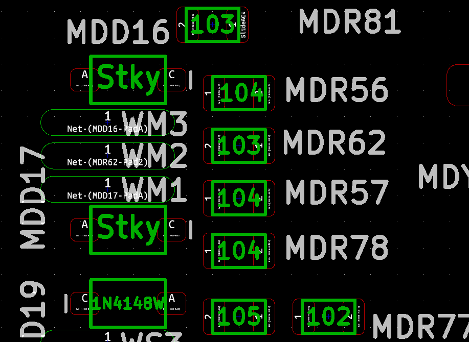
I also had to decide what arrangements my library components would have concerning where the cursor appears relative to a text item when moving it. In my PCB design I had made some such items place the cursor at the bottom left of the text, with this text in bold at the end of some fp_text items:
(fp_text reference DJ1 (at -4.4852 3.3936) (layer F.SilkS)
  (effects (font (size 1 1) (thickness 0.15)) (justify left bottom))
I am not sure how they got this way, since I couldn't find a way in Pcbnew of editing either the justification (left, center or right) or anything to do with top or bottom, using a Windows nightly from 2017-11-18. Editing one of these fp_text items involves a dialogue box:
For free text items (not part of a footprint) there is a way of editing the justification to left, center or right:
Neither of these seem to provide a way of introducing bottom into this part of the PCB file.
For free text items, the "Display:" options are Normal and Mirrored. In the latter case, the PCB file contains:
(justify mirror)
The reasons for this are:
1 -The footprints in my library, as they are made with the techniques described here, have no such justify elements, so the cursor is centred both horizontally and vertically as shown above.
2 - This arrangement is generally best when the footprints are loaded into the PCB design - the fp_text items may be cluttered and on top of each other, but at least they are centred on the component, rather than sticking out in various was as would be the case with left justification.
3 - When a fresh text item is placed in the PCB design, it has these arrangements too.
4 - As noted above, I couldn't find a way in Pcbnew of editing these justify items.
This means that if I have two text items side-by-side, with differing text heights, and want the bottom edge of their characters to line up, then I will need to do some fancy manual editing or place them very finely with a 0.01mm grid, and get them at least this close - ten microns.
So I manually edited my PCB design file to get rid of all such justify constructs.
See a section below for some examples of SMT and through-hole footprints I generated using Library Expert Lite for my KiCad library. Before I could do this, I needed to sort out some other things mentioned in the following sections.
02 - Systematic approaches to naming footprints, based on IPC-7351C
The next question is how to name the
new footprints I generated with the help of Library Expert
Lite. I already have my own names for footprints generated
manually, for specific through-hole pots, switches and connectors - and
there's no need to make their names fit in with any particular scheme
since I am not planning for automated through-hole assembly.
The IPC-7351 standards involve an elaborate scheme for naming footprints. A 2016-10-04 document from PCB Libraries on how PCB Library Expert does - or I guess in earlier versions did - this, according to IPC-7351B, can be found (2017-10-24) in the first PDF link here:
The second link is for a similar document for IPC-7351C, but there is no such file. I found several copies of a 2017-05-17 version IPC-7351C-Land-Pattern-Naming-Convention_.pdf (e.g. link) for IPC-7351C at various other websites. This may not be authoritative, but its the best guide I could easily find. I assume that the current PCB Library Expert Lite implements this naming scheme for every footprint it exports, so I don't need to fuss over the details.
In the above example I used PCB Library Expert Lite to produce a KiCad-format footprint which I believe suits all 0805 chip resistors, based on my choice of dimensions from a data sheet of a major resistor manufacturer. 0805 is the EIA name for such a package, which might be used for resistors, capacitors, inductors etc. The name of the footprint is:
This does not denote the most widely used term for this package, the imperial 0805 or its metric equivalent (https://en.wikipedia.org/wiki/Surface-mount_technology#Rectangular_passive_components): 2012 . I want both these numbers in the footprint name, since I want to be able to think in terms of the EIA package number, while not precluding the use of its metric equivalent.
So for me, once converted to KiCad format, the footprint's name is:
This is rather long-winded, and it is always difficult to try to impose a modicum of order on an intrinsically messy situation without causing unacceptable bloat and further disorder.
This way I can search for i0805 in my footprint library any time I want to find any which match the EIA 0805 package.
#initzerorotationThe IPC-7351 standards involve an elaborate scheme for naming footprints. A 2016-10-04 document from PCB Libraries on how PCB Library Expert does - or I guess in earlier versions did - this, according to IPC-7351B, can be found (2017-10-24) in the first PDF link here:
The second link is for a similar document for IPC-7351C, but there is no such file. I found several copies of a 2017-05-17 version IPC-7351C-Land-Pattern-Naming-Convention_.pdf (e.g. link) for IPC-7351C at various other websites. This may not be authoritative, but its the best guide I could easily find. I assume that the current PCB Library Expert Lite implements this naming scheme for every footprint it exports, so I don't need to fuss over the details.
In the above example I used PCB Library Expert Lite to produce a KiCad-format footprint which I believe suits all 0805 chip resistors, based on my choice of dimensions from a data sheet of a major resistor manufacturer. 0805 is the EIA name for such a package, which might be used for resistors, capacitors, inductors etc. The name of the footprint is:
RESC200X125X60L40N Resistor, chip.
RESC200X125X60L40N Nominal dimensions, mm to two decimal places, leading zeros removed.
RESC200X125X60L40N Nominal lead dimensions.
RESC200X125X60L40N N denotes that this footprint is made according to the Median AKA Nominal density level rules, which concern how much space there is around the component, and the size of the pads. The other options are M for Maximum AKA Most density and L for Minimum AKA Least density.
This does not denote the most widely used term for this package, the imperial 0805 or its metric equivalent (https://en.wikipedia.org/wiki/Surface-mount_technology#Rectangular_passive_components): 2012 . I want both these numbers in the footprint name, since I want to be able to think in terms of the EIA package number, while not precluding the use of its metric equivalent.
So for me, once converted to KiCad format, the footprint's name is:
RESC200X125X60L40N-2012i0805
This is rather long-winded, and it is always difficult to try to impose a modicum of order on an intrinsically messy situation without causing unacceptable bloat and further disorder.
This way I can search for i0805 in my footprint library any time I want to find any which match the EIA 0805 package.
03 - Initial zero rotation for SMT components: IPC-7351C Level A or B?
The .pos file, centroid file or similar by
another name which a PCB designer sends to a PCB assembler contains
rotation angles for each component. In order for this to be
directly useful (without manual checking and potential alteration for
each type of component), the direction of rotation needs to be agreed upon
(anti-clockwise) and the initial zero rotation of each such type of
component needs also to be known at both ends.
Originally there was the IPC-7351 and IPC-7351B standard for zero initial rotation. Then IEC 61188-7 specified some different zero initial rotations for certain classes of component, with this new set being named "Level B" and the original IPC-7351 and IPC-7351B set "Level A". IPC-7351C will be the same as IEC 61188-7 in this regard.
By far the best explanation I know of these standards, and of EIA-481-D (which specifies a third incompatible set of zero rotations for some classes of component), is by Tom Hausherr in 2011:
https://blogs.mentor.com/tom-hausherr/blog/2011/01/14/pcb-design-perfection-starts-in-the-cad-library-part-10/
In the table at the end of this article, columns 2 and 3 correspond to Levels A and B respectively.
Since I think this is a uniquely valuable explanation of a vexed question and since it does not seem to be properly archived at http://archive.org (for instance, here, fig 6 is missing), just in case the original disappears, I have placed a PDF of the article in the directory your browser is now accessing: PCB-Design-Perfection-Starts-in-the-CAD-Library-Tom-Hausherr-2011-IPC7351C-zero-initial-rotation-levels-a-and-b.pdf
As far as I know, Library Expert Lite uses the Level B initial zero rotations, so that is what I will use. I understand the Pro version can produce footprints according to both Level A and B standards. The initial orientation can be changed manually with the the Component tab > Settings sub-tab > Pin 1 Orientation: Left, Up, Right or Down.
I am not aware of any arguments for why Level B is better than Level A. It probably doesn't matter which is used, as long as all components in a single PCB project have their rotations specified to one or the other, and the choice of Level A or B is clearly documented in instructions to the PCB assembly company.
Nor do I know why the second set ("Level B") was created. If anyone has an explanation, the question remains unanswered at: https://electronics.stackexchange.com/questions/84280/why-there-is-ipc-level-a-and-b/ .
#schemsymb
04 - Schematic symbol names
Schematic symbol names don't really
need to fit in with anyone else's standards or ideas of elegance, since
they are of no concern at all to the PCB manufacturer, and are not seen
by the SMT assembly company. Nor are they seen by any other
people or companies who test, repair etc. the equipment I design.
They would be seen by any other person or company for whom I was
working to create said schematics, or two whom I sold or licensed these.
My library is currently small and each symbol is made from scratch or adapted from the main KiCad library or elsewhere, including websites which provide form-based schematic symbol generation.
The symbols fall into several categories:
#validating
My library is currently small and each symbol is made from scratch or adapted from the main KiCad library or elsewhere, including websites which provide form-based schematic symbol generation.
The symbols fall into several categories:
1 - Those that have no footprint at all, such as arrows and power symbols.
2 - Those which represent a construct on the PCB, such as a single pad to which I will solder one strand of a ribbon wire. There is no separate SMT or through-hole component for these, so nothing needs to go onto the final BoMs I generate for purchasing and/or assembly operations. The symbol specifies a particular footprint which does what I want. Since there's no variation in footprint, these symbol names don't need to include anything regarding footprints.
3 - Those which represent a component for the PCB, such as a microcontroller, for which I only ever use a single footprint, so the names of these symbols don't need to include anything regarding footprints.
4 - Symbols for which I don't define a footprint in the library representation of this symbol. This arrangement is how KiCad was designed to be used, by way of CvPcb. However, I will generally fill in the footprint manually when placing such symbols. If I were placing multiple such symbols with the same footprint in a schematic, I would generally place one with a specific footprint, and then copy it, rather than repeatedly manually fill in the footprint of an instance of the symbol just placed from the library.
5 - Symbols for which, for a given electronic function and so matching graphic pattern, have two or more possible footprints and for which I choose to generate separate symbols which look the same, but have the footprint already defined in the library copy of the symbol. Only in this case do I need to think about appending text to the end of the symbol's library name in order to denote which footprint is defined in it. Since I don't need to fit in with international standards, I may will use something simple and widely recognised such as -i0805 . I generally would not want to append the full name of the footprint such as RESC200X125X60L40N-2012i0805.
05 - Validating and fine-tuning the BoM and .pos (centroid) files against the Gerber and drill files, including with VisualPlace
Other pages here ../
concern various ways of creating Bill of Materials files. Here my
interest is in how I fine-tune the creation of these and/or actually
edit or process them in some way that they meet the requirements of a
company which will be doing (or at least quoting on) SMT automated
assembly of a batch of panels, each containing multiple final PCBs, or
PCB sets (for instance, the Devil Fish modifications involve a set of
two separate PCBs, both with fussy shapes created by routing AKA
milling).
I don't at present plan on external assembly companies doing the through-hole components, but there will be a time for that in the future. I assume that such through hole assembly will not be robotic, so there needs to be suitable BoM data and other items such as images depicting component location and orientation - but there is no need for anything like the rigorously correct .pos centroid file as is needed for SMT assembly.
There needs to be fiducial marks, at least on the front (top) of the PCB, as copper circles unencumbered by solder resist, for purposes including the alignment of the solder paste stencil and camera-driven auto-location by the pick-and-place machine. For now I will refer to the SeeedStudio PCB Design for Manufacture document mentioned above #seeestudiodfm , which has extensive notes on local, image and panel fiducials.
Also, from 2013, a widely cited treatise #rghkicaddfm1
Design for Manufacture in KiCad Part 1 – Assembly
explains why fiducials must be represented by schematic symbols, each have reference (RefDes) names of FID1, FID2 etc. and so appear in the BoM and .pos files with those references. I will keep this in mind and consider how it might work in the context of me creating a final design being a panel of multiple boards of the same kind, such as a 3 x 4 array of them, or a 3 x 4 array of the two boards I need. According to SeeedStudios and other things I have read in forums, there needs to be three fiducials for the entire panel, which will all be outside the area of each board, and so can't be part of any ordinary BoM based on a schematic, since there is no schematic for the panel of 12 boards.
Further information on fiducials regarding IPC-5371C can be found in page 27 of #wnipc7351c.
The only thing I have to add to this is that I read on some forums that the single image fiducial (one per functional board in a multi-board panel) has an alternative use to its main purpose of giving the pick-and-place machine more precise location information than it could otherwise get from the three panel fiducials: to be the location of a sticker or some other mark placed by the PCB manufacturer, over the fiducial, to indicate that this board failed electrical test. This can apparently be used by some PCB assembly companies as the signal not to assemble any components on that board. This enables the use of panels with known bad boards, without wasting potentially a lot of money on components and SMT assembly time.
In addition to visual inspection of the images encoded by the various Gerber files (front and back copper, front and back solder mask, front solder paste and front silkscreen) with the holes specified by the drill file, I want to be able to check all that information against the final BoM and .pos files I send to a PCB assembly company.
KiCad's GerbView program enables us to visually check multiple Gerber layers and the holes specified by drill files. It does not handle .pos files.
There is a class of software known as NPI - New Product Introduction - used primarily be PCB assembly companies to handle various kinds of input file, validate the details and produce whatever is required to drive the pick-and-place machines. These input files will include at least some of the Gerber files, I guess the drill files, and especially the .pos (or its equivalent from other EDA packages than KiCad). Here are some names of file types with the same function: to tell the PCB assembly company where each component to be mounted is located. This would be for an individual board, not a whole panel of boards, since the PCB assembly company will use their software to replicate whatever they derive from this, for each board image in the panel.
Some examples of commercial (paid-for licensing, not open-source) NPI software are:
Although I don't need to program pick-and-place machines, I need to be sure the files I send to a PCB assembler contain sufficient and accurate information for them to work on the job with ease.
I am not sure if there are open-source programs which enable me to do this. Please let me know if there are any. (Gerbv is open-source and runs on Linux, but not easily on Windows. It can "display well-formed pick-and-place files", but I think this does not compare with the advanced capabilities of the next program mentioned.)
Good enough for me, however, is free-as-in-beer software, though not open-source - specifically:
VisualPlace is an interactive Windows program which reads Gerber files, one or more drill files and a .pos file, or some other kind of centroid file. It then enables us to check that the positions and orientations of the components, as specified in the centroid file, really match the intended locations.
It doesn't display the components, but it does need to know about their packages, or the footprints presumably correctly designed for them, in order to validate the correctness of the specified position. A section below explores how this program works, but for now, I need to know how fussy it is about the footprint names in the .pos file, since I am planning on using monstrous names for my footprints such as RESC200X125X60L40N-2012i0805 when it has been common practice, with KiCad and other EDA systems, to use footprint names such as 0805 or perhaps R_0805 .
This should work fine, since VisualPlace can be configured to treat any footprint name, from the .pos file, as being equivalent to one of its built-in types, or equivalent to types which can be defined by me the user. The definition is of the centres of the pins, contacts or whatever - the program does not need to know the actual shape of them. It checks that when the set of pin locations is transformed by the X, Y and rotational information in the .pos file, that these land clearly in the middle of the exposed pads it identifies from the Gerber data (for copper, solder paste and solder mask).
This is an enormously useful capability for me. VisualPlace can also be used with user-written plugins, and there is a plugin so that it can drive this set of programs:
which generate the actual files to drive many types of pick-and-place machines. PCBSynergy works from actual EDA design files, not Gerber files, so it is not useful to me for checking Gerbers etc. nor do I have a pick-and-place machine. However, it seems that with these two programs, with a pick-and-place machine, a solder-paste stencil printer, and a reflow oven, one could be up and running assembling PCBs without having to purchase typically expensive software such as those NPI systems mentioned above.
In January 2018 I have not yet used VisualPlace properly. I will do so when I prepare for automated manufacture, hopefully later in 2018.
As mentioned on the KiCad forum (link), here is a free (beer) program which might be helpful for checking the .pos file, which in this context is known broadly as a "pick-list file (PKP)". The forum message explains how to make it work with KiCad.
#footprintnotesI don't at present plan on external assembly companies doing the through-hole components, but there will be a time for that in the future. I assume that such through hole assembly will not be robotic, so there needs to be suitable BoM data and other items such as images depicting component location and orientation - but there is no need for anything like the rigorously correct .pos centroid file as is needed for SMT assembly.
There needs to be fiducial marks, at least on the front (top) of the PCB, as copper circles unencumbered by solder resist, for purposes including the alignment of the solder paste stencil and camera-driven auto-location by the pick-and-place machine. For now I will refer to the SeeedStudio PCB Design for Manufacture document mentioned above #seeestudiodfm , which has extensive notes on local, image and panel fiducials.
Also, from 2013, a widely cited treatise #rghkicaddfm1
Design for Manufacture in KiCad Part 1 – Assembly
explains why fiducials must be represented by schematic symbols, each have reference (RefDes) names of FID1, FID2 etc. and so appear in the BoM and .pos files with those references. I will keep this in mind and consider how it might work in the context of me creating a final design being a panel of multiple boards of the same kind, such as a 3 x 4 array of them, or a 3 x 4 array of the two boards I need. According to SeeedStudios and other things I have read in forums, there needs to be three fiducials for the entire panel, which will all be outside the area of each board, and so can't be part of any ordinary BoM based on a schematic, since there is no schematic for the panel of 12 boards.
Further information on fiducials regarding IPC-5371C can be found in page 27 of #wnipc7351c.
The only thing I have to add to this is that I read on some forums that the single image fiducial (one per functional board in a multi-board panel) has an alternative use to its main purpose of giving the pick-and-place machine more precise location information than it could otherwise get from the three panel fiducials: to be the location of a sticker or some other mark placed by the PCB manufacturer, over the fiducial, to indicate that this board failed electrical test. This can apparently be used by some PCB assembly companies as the signal not to assemble any components on that board. This enables the use of panels with known bad boards, without wasting potentially a lot of money on components and SMT assembly time.
In addition to visual inspection of the images encoded by the various Gerber files (front and back copper, front and back solder mask, front solder paste and front silkscreen) with the holes specified by the drill file, I want to be able to check all that information against the final BoM and .pos files I send to a PCB assembly company.
KiCad's GerbView program enables us to visually check multiple Gerber layers and the holes specified by drill files. It does not handle .pos files.
There is a class of software known as NPI - New Product Introduction - used primarily be PCB assembly companies to handle various kinds of input file, validate the details and produce whatever is required to drive the pick-and-place machines. These input files will include at least some of the Gerber files, I guess the drill files, and especially the .pos (or its equivalent from other EDA packages than KiCad). Here are some names of file types with the same function: to tell the PCB assembly company where each component to be mounted is located. This would be for an individual board, not a whole panel of boards, since the PCB assembly company will use their software to replicate whatever they derive from this, for each board image in the panel.
.pos file. KiCad.
Placement BOM. https://www.smallbatchassembly.com/faq/#Placement-BOM-Format
Component position lists. http://www.techdesignforums.com/...
Placement BOM. https://www.smallbatchassembly.com/faq/#Placement-BOM-Format
Component position lists. http://www.techdesignforums.com/...
Some examples of commercial (paid-for licensing, not open-source) NPI software are:
https://www.mentor.com/pcb/xpedition/npi/ DFM (Design For Manufacture) validation for designers and NPI (New Product Introduction) for PCB assembly companies.
https://www.aiscorp.com/en/operational-excellence/npi-solutions-software NPI and Manufacturing Execution Software.
http://www.unisoft-cim.com/pcbplace.htm "Unisoft ProntoPLACE software translates CAD or Gerber and Bill of Materials (BOM) files into real reference designators, X/Y body centers, Theta rotation, part numbers, etc. This data is then used by Process Engineers to program their SMT and Thru-hole Automatic Assembly Equipment." So this system apparently doesn't require a .pos, centroid or whatever file.
http://www.rssimmons.com/cad_importer/cad_importer.aspx "Converts CAD files from most PCB CAD system into files that can run on your Pick & Place or similar type of machine."
https://www.numericalinnovations.com/collections/fab-3000-gerber-cam Design rule checking, generation of centroid files, panelization and editing of Gerber files. Windows and Linux.
Although I don't need to program pick-and-place machines, I need to be sure the files I send to a PCB assembler contain sufficient and accurate information for them to work on the job with ease.
I am not sure if there are open-source programs which enable me to do this. Please let me know if there are any. (Gerbv is open-source and runs on Linux, but not easily on Windows. It can "display well-formed pick-and-place files", but I think this does not compare with the advanced capabilities of the next program mentioned.)
Good enough for me, however, is free-as-in-beer software, though not open-source - specifically:
VisualPlace is an interactive Windows program which reads Gerber files, one or more drill files and a .pos file, or some other kind of centroid file. It then enables us to check that the positions and orientations of the components, as specified in the centroid file, really match the intended locations.
It doesn't display the components, but it does need to know about their packages, or the footprints presumably correctly designed for them, in order to validate the correctness of the specified position. A section below explores how this program works, but for now, I need to know how fussy it is about the footprint names in the .pos file, since I am planning on using monstrous names for my footprints such as RESC200X125X60L40N-2012i0805 when it has been common practice, with KiCad and other EDA systems, to use footprint names such as 0805 or perhaps R_0805 .
This should work fine, since VisualPlace can be configured to treat any footprint name, from the .pos file, as being equivalent to one of its built-in types, or equivalent to types which can be defined by me the user. The definition is of the centres of the pins, contacts or whatever - the program does not need to know the actual shape of them. It checks that when the set of pin locations is transformed by the X, Y and rotational information in the .pos file, that these land clearly in the middle of the exposed pads it identifies from the Gerber data (for copper, solder paste and solder mask).
This is an enormously useful capability for me. VisualPlace can also be used with user-written plugins, and there is a plugin so that it can drive this set of programs:
which generate the actual files to drive many types of pick-and-place machines. PCBSynergy works from actual EDA design files, not Gerber files, so it is not useful to me for checking Gerbers etc. nor do I have a pick-and-place machine. However, it seems that with these two programs, with a pick-and-place machine, a solder-paste stencil printer, and a reflow oven, one could be up and running assembling PCBs without having to purchase typically expensive software such as those NPI systems mentioned above.
In January 2018 I have not yet used VisualPlace properly. I will do so when I prepare for automated manufacture, hopefully later in 2018.
As mentioned on the KiCad forum (link), here is a free (beer) program which might be helpful for checking the .pos file, which in this context is known broadly as a "pick-list file (PKP)". The forum message explains how to make it work with KiCad.
06 - Some notes on making my own footprints
These are for my own future reference
at least. Perhaps someone else will be interested in them.
Some of the images below show text sizes larger than those which result
from my final way of producing footprints: pasting the block #blocktopaste over the existing fp_text items, which sets the text sizes to 0.80mm.
I made an (imperial) 1206 footprint using the same technique as described above. After the editing described above, the results were KiCad footprints I called:
I also wanted capacitor footprints like these, and since, as far as I can see, the choice of Resistor or Capacitor makes no difference to the footprint generated by Library Expert Lite (it just changes the first characters of its name), I renamed these footprints to capacitor versions, by changing the name of their files and their name and description at the start of the files:
For axial (imperial) 0.3" and 0.4" lead spacing (300 mil and 400mil, for 1/8 and 1/4 watt resistors, respectively) I used the following settings in black. I probably should have used 0.5mm for the 0.3" wire thickness, but I am wary of too-small holes and pads. The results are in green:
I made an (imperial) 1206 footprint using the same technique as described above. After the editing described above, the results were KiCad footprints I called:
RESC200X125X60L40N-2012i0805
RESC320X160X60L50N-3216i1206
RESC320X160X60L50N-3216i1206
I also wanted capacitor footprints like these, and since, as far as I can see, the choice of Resistor or Capacitor makes no difference to the footprint generated by Library Expert Lite (it just changes the first characters of its name), I renamed these footprints to capacitor versions, by changing the name of their files and their name and description at the start of the files:
CAPC200X125X60L40N-2012i0805
CAPC320X160X60L50N-3216i1206
CAPC320X160X60L50N-3216i1206
For axial (imperial) 0.3" and 0.4" lead spacing (300 mil and 400mil, for 1/8 and 1/4 watt resistors, respectively) I used the following settings in black. I probably should have used 0.5mm for the 0.3" wire thickness, but I am wary of too-small holes and pads. The results are in green:
0.3" 0.4"
e Pitch 7.62 10.16
A Max height 1.80 2.20
b Lead diameter 0.60 0.60
D Body length 3.60 6.00
E Body diameter 1.80 2.20
Hole diameter 0.80 0.80
Pad diameter 1.20 1.20 << I changed it to 1.40
e Pitch 7.62 10.16
A Max height 1.80 2.20
b Lead diameter 0.60 0.60
D Body length 3.60 6.00
E Body diameter 1.80 2.20
Hole diameter 0.80 0.80
Pad diameter 1.20 1.20 << I changed it to 1.40
If these calculated hole and pad diameters had been unsatisfactory, I could have set them as I wish with Library Expert Lite's Footprint tab > Dimensions sub-tab. I did this with the pad size for the 0.4" footprint.
I want footprints for two AVX tantalum capacitors:
I can make footprints for these using the Surface Mount > Molded Body > Capacitor, Polarized option, using these numbers I spent about half an hour extracting from the above datasheet, keying into the program and double-checking:
The AVX datasheet did not provide body length, so I used the full length (the terminals stick out a little) minus 0.40mm. For the first of these capacitors:
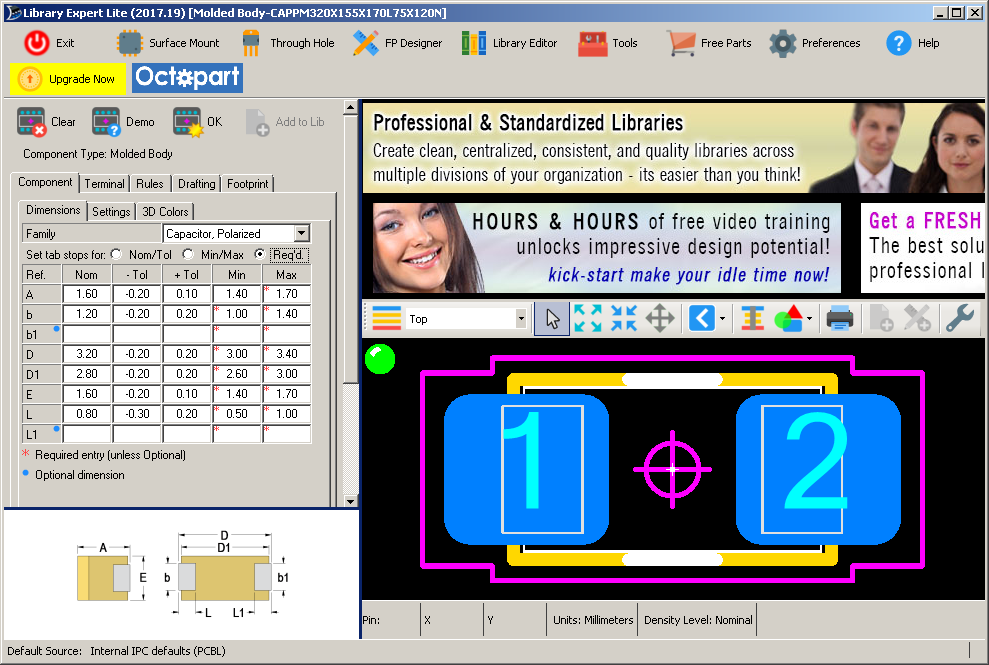
This is missing the polarity indication on the silkscreen layer.
I turned this on with a check box (off by default, every time the program is started) with Drafting tab > Legend sub-tab > Autogenerate Pin 1 Indicator Line.
Referring to the IPC5371C-compliant Library Expert Through-hole Families.pdf, this doesn't show how the polarity indicator should appear. However, page 20 of #wnipc7351c shows capacitor polarity being indicated by a dot. However, the Library Expert Lite 2017-19 does it with a bar with the change just described:
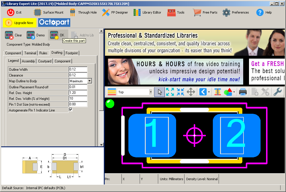
or, by turning off that check box and giving a 0.5mm maximum for the "Pin 1 Dot Size (not to exceed)", I can have dot:
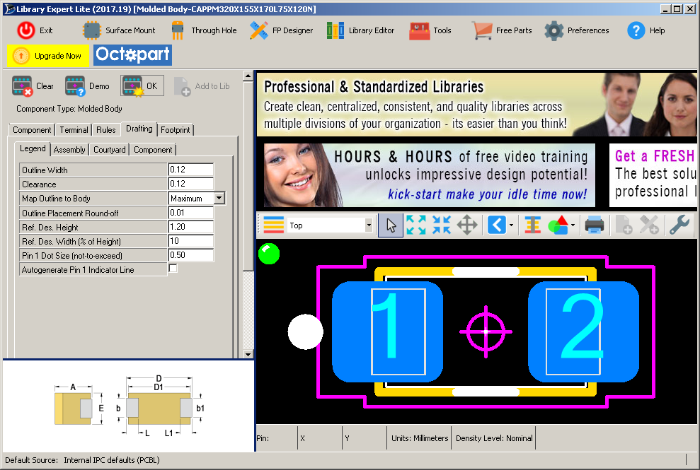
Having a dot or a line is not ideal, I think. SMT tantalum electrolytic capacitors have a line on the case for the positive terminal, while SMT alumimium capacitors, which have different packages, have a line for the negative on the case. I edited my footprints in Footprint Editor to have a new fp_text item with a single character '+', located near pin 1, but not over the pad. This is easy to move around on the PCB design to suit local conditions.
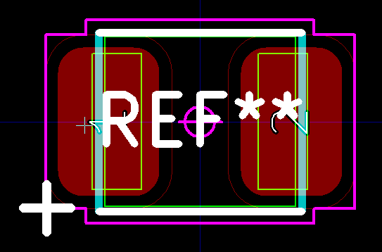
If and when I do aluminium electrolytics, I will do the same thing. A '+' character is unambiguous. A line or a dot could be interpreted to mean all sorts of things, with a line potentially being understood as denoting negative.
I want footprints for two AVX tantalum capacitors:
http://www.avx.com/products/tantalum/smd-tantalum-mno2/taj-series/
http://datasheets.avx.com/TAJ.pdf
http://datasheets.avx.com/TAJ.pdf
0.33uF 35V TAJA334K035RNJ Case A EIA metric: 3216-18
3.3uF 20V TAJB335K020RNJ Case B EIA metric: 3528-21
3.3uF 20V TAJB335K020RNJ Case B EIA metric: 3528-21
I can make footprints for these using the Surface Mount > Molded Body > Capacitor, Polarized option, using these numbers I spent about half an hour extracting from the above datasheet, keying into the program and double-checking:
Library
Expert
AVX 3216-18 3528-21
Tolerance
column column
A Height H 1.60 1.90 +0.20 -0.10
b Terminal width (Y) W1 1.20 2.20 +0.20 -0.20
D Length inc. terminals (X) L 3.20 3.50 +0.20 -0.20
D1 Length body (X) ?
E Width (Y) W 1.60 2.80 +0.20 -0.10
L Terminal length (X) A 0.80 0.80 +0.30 -0.20
column column
A Height H 1.60 1.90 +0.20 -0.10
b Terminal width (Y) W1 1.20 2.20 +0.20 -0.20
D Length inc. terminals (X) L 3.20 3.50 +0.20 -0.20
D1 Length body (X) ?
E Width (Y) W 1.60 2.80 +0.20 -0.10
L Terminal length (X) A 0.80 0.80 +0.30 -0.20
The AVX datasheet did not provide body length, so I used the full length (the terminals stick out a little) minus 0.40mm. For the first of these capacitors:
This is missing the polarity indication on the silkscreen layer.
I turned this on with a check box (off by default, every time the program is started) with Drafting tab > Legend sub-tab > Autogenerate Pin 1 Indicator Line.
Referring to the IPC5371C-compliant Library Expert Through-hole Families.pdf, this doesn't show how the polarity indicator should appear. However, page 20 of #wnipc7351c shows capacitor polarity being indicated by a dot. However, the Library Expert Lite 2017-19 does it with a bar with the change just described:
Having a dot or a line is not ideal, I think. SMT tantalum electrolytic capacitors have a line on the case for the positive terminal, while SMT alumimium capacitors, which have different packages, have a line for the negative on the case. I edited my footprints in Footprint Editor to have a new fp_text item with a single character '+', located near pin 1, but not over the pad. This is easy to move around on the PCB design to suit local conditions.
If and when I do aluminium electrolytics, I will do the same thing. A '+' character is unambiguous. A line or a dot could be interpreted to mean all sorts of things, with a line potentially being understood as denoting negative.
Digression on why many people will be happy to pay for the Pro version of Library Expert
Though this is an explanation of how to use the free (LITE) version, it is
probably a good advertisement for the benefits, for heavy users, of the
Pro version, which has a perpetual license and does not require any
Internet connection to run.
This business of looking up datasheets and manually entering dimensions and tolerances manually is time-consuming and error-prone - especially since the layout and terminology of the information on the datasheet is typically unrelated to that of the program, and because the datasheet may not have all the information.
Furthermore, since the Lite version doesn't remember manual settings such as I made above to generate a polarity indicator line or dot, I would need to remember to set these every time I use the program for any component which needs such settings.
The free version of the program does allow us to create standards compliant footprints and export them to KiCad and other EDA systems, but anyone who has a lot of footprints to make will have a serious impetus to purchase the full version of the program, which, I understand, enables the very rapid generation of footprints, according to local preferences, just by looking up a part number. There is a 2013 explanation for why this powerful, though unsuitable for large-scale use, set of features is made available for free.
#ipc2015le
Digression on an older version of Library Expert which had a part number lookup database with initial settings for the footprint generation process
There used to be a particular version of this program available for free from http://www.ipc.org which I used in early 2016 and wrote about in #thread01. (None were available in October 2017.) For instance see this http://archive.org record of a page (2016-04-08 to 2016-05-18) which linked to a free (and not archived) Library_Expert_IPC-121515.zip. Later snapshots of this page show it linking to zip files with other names, such as Library-Expert-IPC-2016-07.zip.
This zip file Library_Expert_IPC-121515.zip (I downloaded a copy on 2016-02-21 - it has 20,705,867 bytes) includes an installer Install_LibraryExpert2015_17_IPC.exe (20,837,680 bytes, 2015-09-09) which installs (by default in C:\Program Files (x86)\PCB Libraries\Library Expert 2015 IPC\) an executable FPX_2015_IPC.exe which has some capabilities I found useful. It identifies itself (top of window) as "Library Expert for IPC". Here I compare it, as "LE_2015_17_IPC" with the current (October 2017) version which I refer to as "LE_LITE_2017_19".
This zip file Library_Expert_IPC-121515.zip (I downloaded a copy on 2016-02-21 - it has 20,705,867 bytes) includes an installer Install_LibraryExpert2015_17_IPC.exe (20,837,680 bytes, 2015-09-09) which installs (by default in C:\Program Files (x86)\PCB Libraries\Library Expert 2015 IPC\) an executable FPX_2015_IPC.exe which has some capabilities I found useful. It identifies itself (top of window) as "Library Expert for IPC". Here I compare it, as "LE_2015_17_IPC" with the current (October 2017) version which I refer to as "LE_LITE_2017_19".
- LE_2015_17_IPC installs and runs fine without any Internet
connection, while LE_LITE_2017_19 continually communicates with a
license server and will halt if it cannot be reached.
- LE_2015_17_IPC has no footprint export function, as far as I
know. There is no spanner button in the footprint display
window's toolbar.
- Both programs creates a "Libraries" directory in their
installation directories. In an LE_LITE_2017_19 installation this
contains a 120 page PDF file (2016-11-02) with about 5,000 footprints
listed by name, physical description, case code and manufacturer.
This is a list of what is available for free with the Pro version of
the program. In an LE_2015_17_IPC installation, there is no PDF file,
but this directory contains four .fpx files, for through hole, surface mount, BGA and "Sample". The largest, SM.fpx,
contains information for 3,102 surface mount components. These
are text files and the data can be read as described below to set up the
LE_2015_17_IPC with all the measurements and tolerances required to
generate a footprint.
- With LE_LITE_2017_19, if I click the "Preferences" button on the
top toolbar, a web browser window opens with information about the Pro
version. With LE_2015_17_IPC, a window opens which enables me to
set many preferences, though I have not looked at them closely, and
some are grayed out.
- With LE_LITE_2017_19, if I click the "Library Editor" button on
the top toolbar, a web browser window opens with information about the
Pro version. With LE_2015_17_IPC, a window opens which, after 30
seconds or so is populated by a spreadsheet-like set of rows and
columns, which evidently represent the totality of information found in
the .fpx files. There are buttons for importing and opening .fpx
files. Most importantly, the data can be searched with the Find
button and the List All option, so, for instance, I could display only
those lines which contained "3216".
Double-clicking one of these lines caused the Library Editor window to become just part of the whole program's window, and the selected footprint's details would then be displayed, together with the filled in details of component dimensions and tolerances which created it. For instance, for the footprint labeled CAPPM3216X120, which is described as "Capacitor, Polarized, Molded Body; 3.20 mm L X 1.60 mm W X 1.20 mm H body" and as being the "S CASE" according to this Kemet datasheet . I have a visible, but not exportable, footprint and the component dimensions which are the starting point for the program's calculations which produce this footprint. The white silkscreen pattern is an older and bulkier arrangement than the two lines which are produced by the current version of the program, and which are presumably IPC-7351C-compliant.
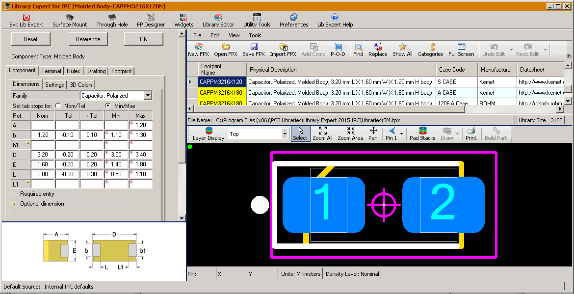
If I can find the component I want in the library list, or one which has the same dimensions as the actual component I am designing for, then this is in some ways a faster way of getting the figures I want. But note that there is no D1 row, as in the current version of the program - and I still need to manually enter these numbers, which takes time and may introduce errors.
Back to my notes on footprints.
For axial diodes I altered the default Component tab > Settings sub-tab > Pin 1 Pad Shape (Pin 1 shape applies only to polarized components) of Square to Round. I also turned on, as described above, the line to indicate polarity, which winds up on the cathode lead. Here is the outcome, for a 0.25" lead spacing diode (such as a BAT85), with the normal 0.3" spacing (1N4148) being the same but a little longer. Here I have moved the REF** text out of the way, but in the library footprint it is located centrally. The F.Fab and Dwgs.User layers are not being rendered so we see the pads (1.2mm diameter, 0.8mm hole), the front courtyard F.CrtYd in magenta and the silkscreen F.SilkS in white:
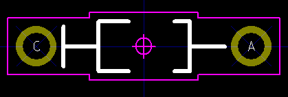
For a 28 pin DIP (0.3" spacing) socket, with square hole for pin 1 and with the "polarity line" turned on, there is no actual line for pin 1, but the presence and absence of certain lines on the silkscreen layer. I decided this was rather cryptic and that a dot was better.

The name Library Expert Lite 2017-19 assigned to my creation was: DIPS762W60P254L3550H430Q28. At this point I spat the dummy. (North Americans: read "pacifier".) This socket is not going to be mounted automatically since it is not SMT. So I don't need to worry much about how this footprint name works with SMT centroid file validation software such as VisualPlace. This name is way-too long and cryptic, so I called my footprint:
DIP28N-Socket
I edited the legend lines to provide a familiar curved notch, rather than rely on the small dot and the missing lines, so this maintains a ~50 year old tradition. I also changed the 1.2mm pads to 1.32MM to match those I used in the past:
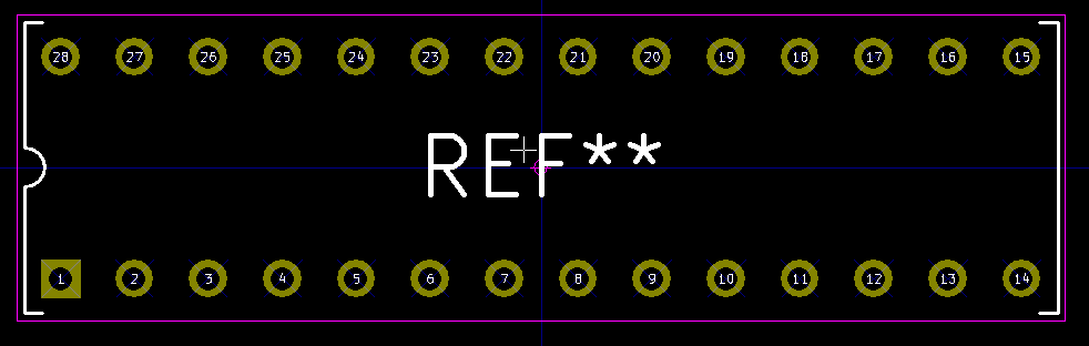
For a Multicomp (element14 house brand) crystal
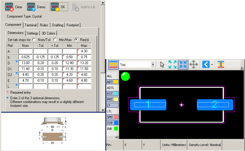
I tolerated the generated name for this: XTAL1140X470X430D1300L430X62N and added -HC49-US to the end for the benefit of mortals.
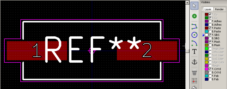
Here are my settings for SOIC 16, with
the numbers retrieved from a TI datasheet. After reading about
the details of the various SOIC standards: https://en.wikipedia.org/wiki/Small_Outline_Integrated_Circuit#JEDEC_and_EIAJ_standards
I recognised that this is a JEDEC size, with the body being ~3.8mm
wide. There are also EIAJ SOICs with ~5.3mm wide bodies. If
I ever need these I will put an E at the end of the footprint
name. In 16 pins only, there is also a JEDEC wide size, with 7.4 to
7.8mm wide bodies, as used in the remarkable ADuM4160 USB isolator.
The only other setting I changed was in the Drafting tab > Legend sub-tab where I turned on "Autogenerate Pin 1 Indicator Line". (Before this can be set, the values must be filled in to the program's satisfaction and the OK button clicked. After this change, the green dot turns red and it is necessary to click the OK button again. This needs to be re-done every time a footprint is exported and new dimensions are entered.)
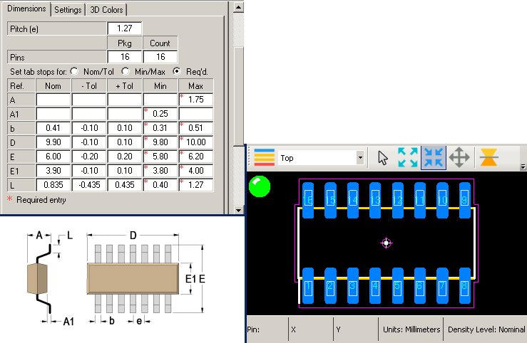
The program's default name for this footprint was SOIC16P127_990X600X175L83X41N which I deemed to be too long. I called it SOIC-16. By changing a few numbers according to the above-mentioned Wikipedia article, I created JEDEC sized footprints SOIC-8, SOIC-14 and SOIC-16W.
SOT packages are all over the place, with different pitches and numbers of pins. I entered these details based on a Fairchild datasheet for BC847CMTF. The only figure not on the datasheet was L max, so I copied the 0.60 from a similar set of values I found for a TI SOT case from the 2015 version of the program, though I am sure I could have found it in some other manufacturer's datasheet.
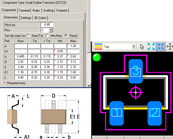
#pcbdfmThe only other setting I changed was in the Drafting tab > Legend sub-tab where I turned on "Autogenerate Pin 1 Indicator Line". (Before this can be set, the values must be filled in to the program's satisfaction and the OK button clicked. After this change, the green dot turns red and it is necessary to click the OK button again. This needs to be re-done every time a footprint is exported and new dimensions are entered.)
The program's default name for this footprint was SOIC16P127_990X600X175L83X41N which I deemed to be too long. I called it SOIC-16. By changing a few numbers according to the above-mentioned Wikipedia article, I created JEDEC sized footprints SOIC-8, SOIC-14 and SOIC-16W.
SOT packages are all over the place, with different pitches and numbers of pins. I entered these details based on a Fairchild datasheet for BC847CMTF. The only figure not on the datasheet was L max, so I copied the 0.60 from a similar set of values I found for a TI SOT case from the 2015 version of the program, though I am sure I could have found it in some other manufacturer's datasheet.
There's no need for a pin 1 indicator line. The program's name for this footprint was rather long - SOT23-3P95_240X120L40X48N
- but I kept it, since I can imagine that in the future I might want to
use could be numerous variations on the "SOT-23 3 pin" package,
which previously, in my ignorance, I thought was a simple and well
standardised thing.
In Footprint Editor I changed the pin names from 1 2 3 to B E C to suit the transistors I am using, though I guess there are variations on this assignment too. (There may be arguments for keeping these as 1 2 3 and numbering the pins of the schematic symbol to match, but I would like to see clear indications of Base, Emitter and Collector on the PCB layout, and in the schematic, I have no real interest in seeing numbers 1, 2 or 3 as pin numbers.)
I can adapt this in Footprint Editor if I want a similar package for a diode. With "REF**" temporarily moved, here are the pads, pin names, silkscreen and, on Dwgs.User, outlines of the pins and body:
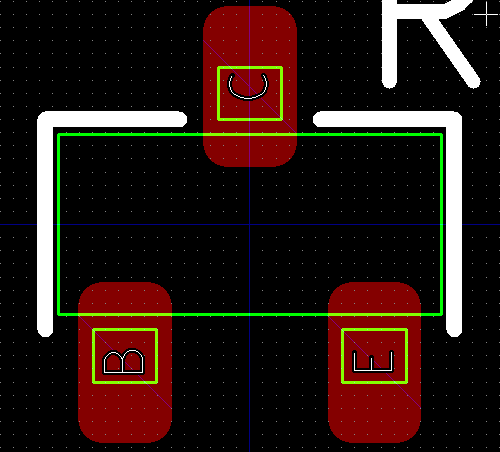
All the footprints I mention in this section were edited as described above before importing them into KiCad's Footprint Editor, after which I saved them to my personal library.
In Footprint Editor I changed the pin names from 1 2 3 to B E C to suit the transistors I am using, though I guess there are variations on this assignment too. (There may be arguments for keeping these as 1 2 3 and numbering the pins of the schematic symbol to match, but I would like to see clear indications of Base, Emitter and Collector on the PCB layout, and in the schematic, I have no real interest in seeing numbers 1, 2 or 3 as pin numbers.)
I can adapt this in Footprint Editor if I want a similar package for a diode. With "REF**" temporarily moved, here are the pads, pin names, silkscreen and, on Dwgs.User, outlines of the pins and body:
All the footprints I mention in this section were edited as described above before importing them into KiCad's Footprint Editor, after which I saved them to my personal library.
06 - Various web pages, forum discussions and documents regarding PCB design for manufacture
I found a detailed treatise on how to
make panels of smaller PCBs which can be snapped out after automatic
SMP assembly, with lots of information on mouse-bites . . . To do: find
it and add the URL here.
When I finalise my PCB design, which is a larger and smaller board set, I will make a panel of six sets with Pcbnew's right click (after selecting the whole layout) Create Array command.
For these prototypes I did this and prepared routing patterns with mouse-bites, based on the advice in:
When I finalise my PCB design, which is a larger and smaller board set, I will make a panel of six sets with Pcbnew's right click (after selecting the whole layout) Create Array command.
For these prototypes I did this and prepared routing patterns with mouse-bites, based on the advice in:
I didn't find out how these worked, since my panel design lacked a proper outer frame and PCBFast explained that it would be best to route (mill) the boards out completely in this case. To do a frame I will need to consult with whoever I choose to do the SMT assembly in order to get their requirements for the frame surrounding the boards, tooling holes and fiducials.
PCBFast's normal routing (milling) arrangement is 2mm, and I prepared outlines for the boards on my ECO2.User layer, for which I generated a Gerber file. I assume they or any other manufacturer has software which uses the tracks on such a Gerber file to program the router to do whatever is needed to achieve boards with these outlines.
One corner of one of the boards looks like this, with a mouse-bite (breakaway) joint holding it to the rest of the panel:
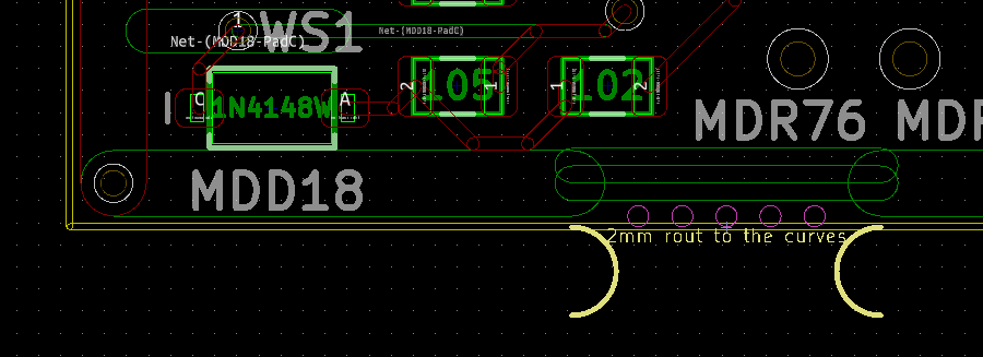
The yellow track defines the outline of the PCB - where I want the router to go to. I didn't break this track at the mouse-bite, but in the future I will. The mouse-bite itself is a footprint, which is in the library zip at the start of this page. It consists of some text and two 2mm diameter semicircles on the ECO2.User layer, with five non-plated through holes.
The idea is that the person at the PCB manufacture company will guide their software so the router stops at the semicircles. If there is a better, more industry-standard, more automatic, way of specifying how to rout (mill) the edges of PCBs, I would like to know about it.
It is my impression that PCB manufacturing companies get all sorts of messy Gerbers from customers and have the software, the skills and the patience to deal with most of it gracefully and reliably. So as long as the Gerber file I give them for my PCB fabrication mechanical layer (ECO2.User) is reasonably clear, I guess things will work out well. The fully separated, routed, boards were precisely as I specified with these tracks. I made the tracks reasonably thin so it wouldn't matter if they used the edge or the centre of these tracks.
Update history:
- 2019-01-02: Initial version.