Data Structures for KiCad - especially for generating BOMs
2017-10-09 Robin Whittle
rw@firstpr.com.au A non-expert's initial attempts at setting up KiCad schematics and schematic libraries to ease tasks including purchasing parts and generating Bill of Materials files for various purposes.
Please see the parent directory for other items regarding KiCad, including links to other sites which may be of interest to anyone concerned with these things, including a link to the KiCad users mailing list: ../#kds .
Contents
| #int |
01 - Intro and goals |
| #files |
02 - The major files in the whole project |
| #incr |
03 - Incremental design with repeated iterations of schematic change, new netlist, read netlist into PCB design |
| #gen |
04 - BoM generation techniques |
| #fields |
05 - Choice of fields to add to schematic components |
| #copying | 06 - Copying one or more components to the same schematic sheet or to a different schematic sheet in the same project |
| #basic |
07 - The basic BoM CSV file |
| #group |
08 - A BoM CSV file with grouping - and a bug fix for the .xls file which creates these |
| #other |
09 - Other approaches to generating BoMs |
01 - Intro and goals
For any PCB project - and especially
for SMT projects to be automatically assembled by some other company -
quite a bureaucracy needs to be designed and maintained to keep
a track of all the components, for a variety of purposes. Below
is my exploration of how to do this, as part of my first KiCad PCB
design project, which is also the first time I have designed using
SMT.
This page contains a detailed account of how I set up my first KiCad project so that at the level of the schematic library components, and the components in the actual schematics, each component has extra fields with various kinds of data to help me achieve:
This page contains a detailed account of how I set up my first KiCad project so that at the level of the schematic library components, and the components in the actual schematics, each component has extra fields with various kinds of data to help me achieve:
- The ability to have a different piece of text, or just a space,
be the Value in the PCB design which is different from the text of the
Value in the schematic. This involves a field PCBVal and processing the netlist file generated by Eeschema with a C++ program kicad-pcb-value
to produce a modified netlist file to be read into Pcbnew. In those
components for which I do not want to make such changes, the value of
the PCBVal field is set so that its first and perhaps only character is '%'. Please see the parent page ../#kpv for details.
- The ability to generate various files, broadly called BoMs (Bills of Materials) for a variety of purposes, including:
- Handling some components for which there is a single perfectly
defined part number, while others might have multiple possible part
numbers and while others still may be specified in a more generic
fashion.
- Ordering parts for our own assembly work, which is preceded by
establishing where a component might be purchased from, at what price
etc. and deciding which orders to make to various suppliers, many of
them in the USA, with consequent delays and freight costs per
order, depending on the value of the order. This requires considering various combinations
of whether to order from each supplier, including Mouser, DigiKey and OnlineComponents in the USA, via element14 or Switches Plus here in Australia. We also order Kingbright LEDs from Tenrod in Sydney and get some other parts from Altronics and X-ON in Perth, RS Components , Jaycar , WES Components in Sydney and RapidOnline in the UK.
- Specifying parts for automated SMT assembly by a company here in Melbourne (https://www.duet.com.au) who will have some of the parts we need in stock, and others which
they may be able to purchase or which we will need to supply.
- In the future, in principle, the system would ideally handle
BoMs suitable for companies we have not yet dealt with who might do
complete SMT and through-hole assembly and test. This would be
preceded by the need to get quotes, which requires detailed BoMs, PCB
and other engineering documents, each set in a format suited to the
particular assembly company.
I also need to generate .pos
files for the pick-and-place (PNP) machine which will be doing the SMT
assembly. I haven't got this far yet, and to what extent this
involves data from the BoM I am not yet sure.
One potential concern is that I have not generated my PCB footprints, in respect of their centering and rotation, with strict adherence to the orientation of the devices in the reels of tape which the PNP machine works from. I understand that component rotation is something typically adjusted and checked by the SMT assembly company so for now I am not fussing about this. See https://rheingoldheavy.com/design-assembly-kicad/ for some guidance on scrutinizing specs for orientation of devices in the reel tape and generating footprints to match.
I can't fully understand all the things I might want to do with data from KiCad projects, so I can't design a totally ideal system now. Nor can I necessarily understand or directly apply the approaches documented by other more experienced users - see sites linked to at: ../#bomwlinks and ../#links . Some of those accounts are based on earlier versions of KiCad, in which there were only field numbers as high as 11 or so for schematic components.
#files
02 - The major files in the whole project
I am using KiCad compiled for Windows -
either the stable release or one of the nightlies - because I found it
difficult to compile for Linux due to the large number of prerequisite
packages (and since in October 2017, the latest version 4.0.7 was only
available in a precompiled form for Debian if I used the Testing
version of Debian, which is not at all convenient for me). My
Windows 7 Dell E6410 laptop is
in a docking station with four 1920 x 1200 monitors. Two of these
are driven by USB adaptors
with DisplayLink chips. So I can have numerous programs open and
visible all at once.
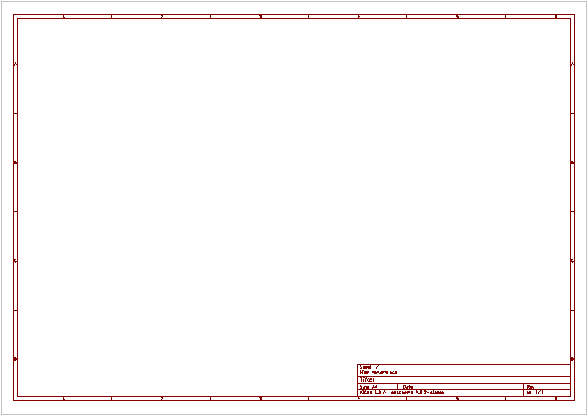
I run the KiCad program and from this run Eeschema and Pcbnew. This enables linkage so that selecting a component in a schematic open in Eeschema causes Pcbnew to scroll to wherever that component's footprint is in the PCB design. I used the KiCad program's Tools > Run Page Layout Manager to create a new border and title block file which I configured my main schematic (and therefore those hierarchically under it) to use. This extends the border box a little closer to the edge of the A4 sheet and reduces clutter to give more space for circuitry. This one file works for any page size. In both Eeschema and Pcbnew, it can be selected via File > Page Settings:
I have my own single library of schematic components, two files D:\PCB\Kicad\RW-component\0RW.dcm and 0RW.lib. The actual component data is in the .lib file and the text descriptions are in the .dcm file. I generate my own components from scratch, start with one copied from the GitHub libraries, or generate them from the excellent online program for creating KiCad components with lots of pins: http://kicad.rohrbacher.net/quicklib.php , which can work from a text file of pin numbers and names.
I have a single library of PCB footprints - a directory of "module" files, one for each footprint: D:\PCB\Kicad\RW-footprint\RW-Footprint.pretty . Please see ../#smtf for notes on how I attempted to make SMT footprints in accordance with standards and knowledge from experienced people. This is my first attempt at SMT design.
There is a master schematic file with several further files as part of the one schematic project with its own .pro project file. These schematics are linked hierarchically, as described in the Eeschema User Manual: http://kicad-pcb.org/help/documentation/#_eeschema. These are in the same directory as the single Pcbnew PCB file. Netlist files are created in this directory by Eeschema and a new version of the netlist file is created, also in this directory, with my kicad-pcb-value program. I have a sub-directory for Schematic plots and another for PCB plots. (File > Plot > PDF.)
I regularly back up the library directories and the important files from this project directory to a series of 100 directories on another machine. This was hard to do manually, so I created a batch file and file list file (here they are as an example) to drive the 7za.exe 7-ZIP Extra command-line version of 7Zip to create a .7z archive which I manually copy into the next one in sequence of these 100 directories. (The KiCad program has an archive command to do much the same thing - zip up all the files and sub-directories of the project directory, with the File > Archive command, with a matching button for this on the top toolbar.)
#incr
03 - Incremental design with repeated iterations of schematic change, new netlist, read netlist into PCB design
KiCad is documented as if the designer
wants to create a generalized schematic, where each component has no
particular footprint associated with it. In this method of using KiCad, once the schematic is
finished, a separate program CvPcb is run to fill in the footprint fields
of all the schematic components. This is done according to
"Footprint Filter" text items which are also part of each component's
internal data (both in their library representation and as components
in a schematic). This has the advantage that the one schematic
can be made to create multiple PCBs depending on the choice of
footprints, where such a choice is possible - as it frequently is for
small resistors, or between DIP and SOIC versions of chips.
I am one of the many KiCad users who don't want to work this way since I know the package I want for all components when I am creating the schematic. All my schematic components (in the schematic libraries and as components in schematics) have nothing in their Footprint Filter section. Their Footprint field is always filled in with one precise footprint specification, which takes the form of the nickname (in Pcbnew's library configuration) of the footprint library (I have only one library for all the footprints I use), followed by a colon, followed by the name of the footprint in that library:
I am designing the project incrementally. For each major cycle I create one section's schematic, generate a netlsist ("NET" button on Eeschema's top toolbar), process it with kicad-pcb-value (../kpv) to generate a modified netlist and then read this netlist into Pcbnew ("NET" button on top toolbar), with the Netlist options (Tools > Netlist > Read Current Netlist) set so that footprints already in the design will be replaced by matching footprints specified in the netlist (Exchange Footprint > Change) or will not be (Exchange Footprint > Keep). I am still figuring out which of these options I want, depending on the nature of the changes I am making. This selection seems to default to "Keep".
My system does not so far use the back-annotation capabilities of KiCad, in which changes of some kinds in Pcbnew are propagated to the schematic. There seems to be little documentation of this (Eeschema manual 4.8.1) and I have not yet figured out how it works, or whether it would be useful.
I also have some of the footprints locked in position so I can't accidentally move or edit them.
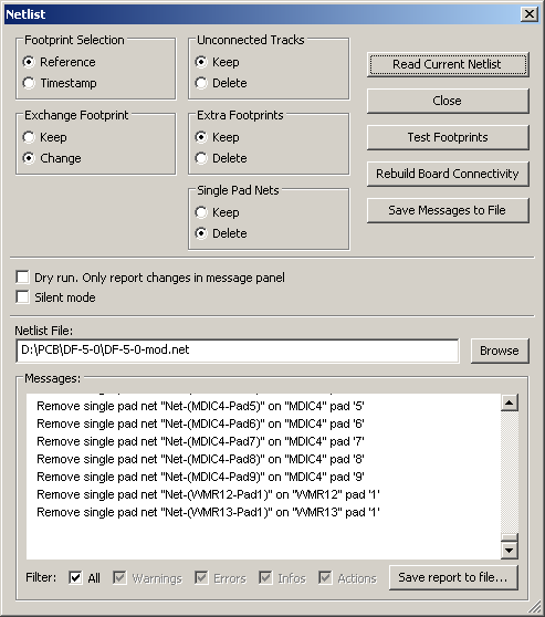
This "Read Current Netlist" operation adds a bunch of footprints outside the board's perimeter, all in the one place. I click the Footprint Mode icon in the top toolbar so it is activated - as shown below by having a box around it:
I am one of the many KiCad users who don't want to work this way since I know the package I want for all components when I am creating the schematic. All my schematic components (in the schematic libraries and as components in schematics) have nothing in their Footprint Filter section. Their Footprint field is always filled in with one precise footprint specification, which takes the form of the nickname (in Pcbnew's library configuration) of the footprint library (I have only one library for all the footprints I use), followed by a colon, followed by the name of the footprint in that library:
I am designing the project incrementally. For each major cycle I create one section's schematic, generate a netlsist ("NET" button on Eeschema's top toolbar), process it with kicad-pcb-value (../kpv) to generate a modified netlist and then read this netlist into Pcbnew ("NET" button on top toolbar), with the Netlist options (Tools > Netlist > Read Current Netlist) set so that footprints already in the design will be replaced by matching footprints specified in the netlist (Exchange Footprint > Change) or will not be (Exchange Footprint > Keep). I am still figuring out which of these options I want, depending on the nature of the changes I am making. This selection seems to default to "Keep".
My system does not so far use the back-annotation capabilities of KiCad, in which changes of some kinds in Pcbnew are propagated to the schematic. There seems to be little documentation of this (Eeschema manual 4.8.1) and I have not yet figured out how it works, or whether it would be useful.
I also have some of the footprints locked in position so I can't accidentally move or edit them.
This "Read Current Netlist" operation adds a bunch of footprints outside the board's perimeter, all in the one place. I click the Footprint Mode icon in the top toolbar so it is activated - as shown below by having a box around it:
Then I right click anywhere on the screen, which generates a menu from which I use: Global Spread and Place > Spread out Footprints not Already on Board. Then the components are within the board's boundaries and each one is in a different location. After this I can move them around, guided by the white ratsnest rubber-band like lines. Then I manually place tracks to satisfy the net connections signified by the ratsnest. I typically have to revise or make new schematic library components and footprints while doing this.
If I have placed multiple footprints and want to change them, I use the footprint library editor to make the modified footprint of the same name. Then, for one of the footprints in the design with that name, I edit the parameters (pressing E while the cursor is over the footprint is one way of doing this), which leads to a dialogue box with a "Change Footprint(s)" button at the top right. This marvel enables me to replace the currently edited footprint, or all footprints with the same footprint name, with the footprint of this name from the currently selected footprint library. This automagically replaces them in-situ, leaving their text items as they were set, in their current positions.
Some schematic components have multiple symbols, one for each section of the library component, representing separate functional blocks within the physical device. For instance, for the 4053 triple 2:1 analog multiplexer (here is the component, exported from the library editor: 4053-soic.lib.txt and 4053-soic.dcm.txt) :
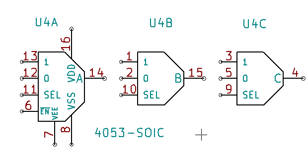
I think that the fields referred to below for part number, stock numbers etc. probably only need to be filled in for the first section (A) of multi-section components such as this, but I am yet to confirm this.
I create the schematic by arbitrarily assigning sections of the 4053 to particular parts of my circuit. However, when placing the footprint in the PCB, for the entire chip, and when placing tracks to satisfy the net connections resulting from this particular schematic, I may decide I want to swap sections or otherwise rearrange the sections with respect to their circuit functions. This applies within a single physical chip like this, or between multiple sections in multiple 4053s.
So I make the changes in the schematic, by moving the symbols without dragging their connections. Then I create a new netlist, create a modified version with kicad-pcb-value, read this into Pcbnew, and the ratsnest of yet-to-be-satisfied-by-copper-tracks connections now follows the new assignment of section to circuit function.
This process is repeated many times:
- Change the schematic in some way, perhaps adding components, but
more frequently changing something like section assignments, pin
numbers and names or whatever. The change might be as small as to
alter the value of a PCBVal
field in one component.
- Generate a new netlist and a modified version of it with my program ../kicad-pcb-value/ .
- Read the modified netlist into Pcbnew.
- Continue working with footprint placement, laying tracks, moving text, checking things etc.
In principle, all the schematic components in the schematics are the same as those of the same name in the schematic library, not counting necessary changes for the individual and now real nature of the components as part of a schematic. Likewise, all the footprints on the PCB should be identical to those in the footprint library.
#gen
04 - BoM (Bill of Material) generation techniques
It is possible to generate a BoM file
from Pcbnew. However, this won't have all the information such as
manufacturer's part numbers, supplier order codes (SKUs) etc. which can
and should be encoded into the fields of the Eeschema schematic
components, at the schematic and library levels.
The basic, built-in, method of generating a BoM file from Eeschema 4.0.7 running under Windows 7 is documented here: ../#bomw . Below (#group), I explore a modified version of this technique to generate such a file with multiple instances of the same type of physical part grouped (AKA collated, combined or whatever) into a single line of the BoM CSV file.
In another page I explore the Python BOM generating scripts which were included with KiCad 4.0.7: ../kicad-python-bom-scripts/ .
It is also possible to generate a BoM by having a program process the schematic files themselves. In principle it would be possible to generate a BoM by processing the netlist file, since it contains all the field data, and is generated as a single file from potentially multiple hierarchically linked schematic files.
#fields
05 - Choice of fields to add to schematic components
I don't want to have to rework the
entire component library later when I find out I need some new
field. Yet I don't have the experience to know exactly what data
I will need in the long-term future. Here is what I chose to add
to all the components in my schematics and schematic library, not
counting those which are power symbols or arrows (I made these power
symbols, and they have no pins). Hopefully this will be
sufficient for this first project.
| Field name |
Purpose |
| PCBVal |
If the contents (the "value") of this field do not start with the '%' character, the contents will written by
the kicad-pcb-value program ../kicad-pcb-value/ into the Value field of this footprint in
the modified netlist file, so this new text is read into the Value
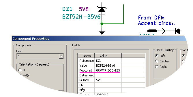
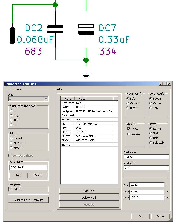
field of the footprint in the PCB design. The value of this field, like that of any other field, can appear in the schematic if the "Visibility > Show" tick-box is ticked the component editor. In an image below, the values 683 and 334 are both set to be visible for their components DC2 and DC7. |
| PN |
One or perhaps more part
numbers. This and all the other fields can be made visible on the
schematic, but usually I leave them invisible. |
| Mfg |
Manufacturer's
name - or potentially multiple such names. This is also a place
where I might add notes. I may list a local distributor here, if
that is where I frequently buy the parts from. |
| SN-e14 |
Stock number, order code, SKU or whatever for element14. |
| SN-MO |
Likewise for Mouser. |
| SN-DK | Likewise for DigiKey. |
| SN-OC | Likewise for OnlineComponents. |
For instance, here is an edit component dialogue box for DC7, showing the contents of many of these fields.
No doubt other fields could be added. Other people have fields for links to distributor web pages, a pair of fields for stock number and preferred distributor and another pair of these for a secondary distributor. I have not used the Datasheet field, which is a standard field of KiCad.
I initially added these fields by text editing the schematic file and the schematic library .lib file. This has some advantages over what would be the more usual way, which is to configure Eeschema to have these fields - each with a suitable default value (text content) and default visibility flag - in the Template Field Names section. Please see ../#tfn for details on how to do this.
I am using 4.0.7 for the actual work. With this version's Eeschema, the Preferences > Schematic Editor Options > Template Field Names section looks like this:
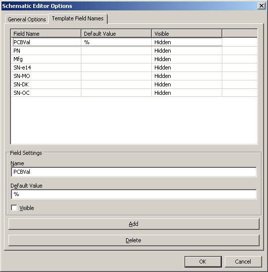
when set up to make all the fields in the table above become part of every component which is edited, either in the schematic itself or in the schematic library.
When Eeschema is closed, this information is saved as a line in Eeschema's config file. So this affects all projects, and is not stored in the project files. When installing a new version of the KiCad programs, it is possible that this information will not be retained, so it would be a good idea to first save the config files to somewhere else before installing a new version. The line in the Eeschema config file which represents the above data is (with each but the last line end below representing a space):
On my Windows 7 Prof 64 bit system with KiCad 4.0.7, the config files for the various programs are found in:
There can be quite a lot of information to add when filling in the values of at least some of these fields - and this is typically added after the component has been placed in the schematic, with its original field values identical to those in its representation in the schematic component library. For instance, I have one schematic library component for unpolarized capacitors with a particular footprint. The fields for all instances of this component in the schematic, for 0.1uF where the capacitance must be stable will be a particular part number or several alternative part numbers, and their stock numbers. For a 0.01uF capacitor these would be different. For a 0.1uF power supply bypass ceramic capacitor with the same footprint where the tolerance is not so tight, this would be some generic ceramic multilayer capacitor, with different part numbers etc.
It would be slow and error-prone to place a library component, edit multiple fields for it to be a 0.1uF stable capacitance type, and then do it again and again for multiple such components.
One approach to reducing data input effort and errors would be to create library components for each such type and value of capacitor - but that would be unwieldy.
The best approach seems to be to filling the details for the first instance of a particular component in the schematic (or in one of the schematics in a hierarchical schematic project), such as 0.1uF small tolerance, high stability, voltage = X unpolarized capacitor with a particular footprint, and then copy from the first instance of such a component to create a second and subsequent instance, with all the same values in the appropriate fields, rather than placing the second or subsequent one from the library as was necessary for the first instance and having to fill in the fields' values all over again.
Copying blocks of components, including just one component, within the one schematic or to another schematic in the same project, is the subject of the next section.
No doubt other fields could be added. Other people have fields for links to distributor web pages, a pair of fields for stock number and preferred distributor and another pair of these for a secondary distributor. I have not used the Datasheet field, which is a standard field of KiCad.
I initially added these fields by text editing the schematic file and the schematic library .lib file. This has some advantages over what would be the more usual way, which is to configure Eeschema to have these fields - each with a suitable default value (text content) and default visibility flag - in the Template Field Names section. Please see ../#tfn for details on how to do this.
I am using 4.0.7 for the actual work. With this version's Eeschema, the Preferences > Schematic Editor Options > Template Field Names section looks like this:
when set up to make all the fields in the table above become part of every component which is edited, either in the schematic itself or in the schematic library.
When Eeschema is closed, this information is saved as a line in Eeschema's config file. So this affects all projects, and is not stored in the project files. When installing a new version of the KiCad programs, it is possible that this information will not be retained, so it would be a good idea to first save the config files to somewhere else before installing a new version. The line in the Eeschema config file which represents the above data is (with each but the last line end below representing a space):
FieldNames=(templatefields
(field (name PCBVal)(value %)) (field (name PN)) (field (name
Mfg)(value " ")) (field (name SN-e14)(value " ")) (field (name
SN-MO)(value " ")) (field (name SN-DK)(value " ")) (field (name
SN-OC)(value " ")))
On my Windows 7 Prof 64 bit system with KiCad 4.0.7, the config files for the various programs are found in:
C:\Users\Robin\AppData\Roaming\kicad\eeschema
fp-lib-table
kicad
kicad_common
pcbnew
fp-lib-table
kicad
kicad_common
pcbnew
There can be quite a lot of information to add when filling in the values of at least some of these fields - and this is typically added after the component has been placed in the schematic, with its original field values identical to those in its representation in the schematic component library. For instance, I have one schematic library component for unpolarized capacitors with a particular footprint. The fields for all instances of this component in the schematic, for 0.1uF where the capacitance must be stable will be a particular part number or several alternative part numbers, and their stock numbers. For a 0.01uF capacitor these would be different. For a 0.1uF power supply bypass ceramic capacitor with the same footprint where the tolerance is not so tight, this would be some generic ceramic multilayer capacitor, with different part numbers etc.
It would be slow and error-prone to place a library component, edit multiple fields for it to be a 0.1uF stable capacitance type, and then do it again and again for multiple such components.
One approach to reducing data input effort and errors would be to create library components for each such type and value of capacitor - but that would be unwieldy.
The best approach seems to be to filling the details for the first instance of a particular component in the schematic (or in one of the schematics in a hierarchical schematic project), such as 0.1uF small tolerance, high stability, voltage = X unpolarized capacitor with a particular footprint, and then copy from the first instance of such a component to create a second and subsequent instance, with all the same values in the appropriate fields, rather than placing the second or subsequent one from the library as was necessary for the first instance and having to fill in the fields' values all over again.
Copying blocks of components, including just one component, within the one schematic or to another schematic in the same project, is the subject of the next section.
#copying
06 - Copying one or more components to the same schematic sheet or to a different schematic sheet in the same project
KiCad's behaviour is not exactly like a
conventional GUI program, which uses the computer's clipboard and
reasonably standardized concepts of cut, copy and paste.
For instance, if a component in a schematic is selected by clicking on it with the mouse/trackball, it does not appear any different on screen. However, the selection can be seen by the details displayed in a bar near the bottom of the window. Likewise if a track, or a text item is selected.
Since it was not immediately obvious to me how to do it, here is a detailed cheatsheet on copying one or more schematic components, and potentially the connection wires, junctions and any other items which are selected with them..
Copying a single component to somewhere in the same sheet is done like this:
Copying one or more components as a block from one schematic sheet to another schematic sheet in the same project is trickier:
For instance, if a component in a schematic is selected by clicking on it with the mouse/trackball, it does not appear any different on screen. However, the selection can be seen by the details displayed in a bar near the bottom of the window. Likewise if a track, or a text item is selected.
Since it was not immediately obvious to me how to do it, here is a detailed cheatsheet on copying one or more schematic components, and potentially the connection wires, junctions and any other items which are selected with them..
Copying a single component to somewhere in the same sheet is done like this:
- Select the component by left clicking and releasing, with the cursor placed over the component.
If the selection is unambiguous, the selected component will not appear any different, but its details will appear in the bar below the main editing window. If it is ambiguous, such as selecting both a component and a pin of the same component, a pop-up window will appear by which we choose which one we are selecting.
- Press the C key (with or without shift). Now a copy of the
component appears and is moved around as we move the cursor. We
move the copy to a new location (or press Esc if we want to cancel this
operation) and press and release the left mouse/trackball button to place it there.
Copying one or more components as a block from one schematic sheet to another schematic sheet in the same project is trickier:
- Select the one or more components and wires, text etc. by
dragging the cursor (left mouse button down) to make a rectangular
marquee around whatever is to be copied. While still holding the
left button down, with the desired selection complete, the screen will
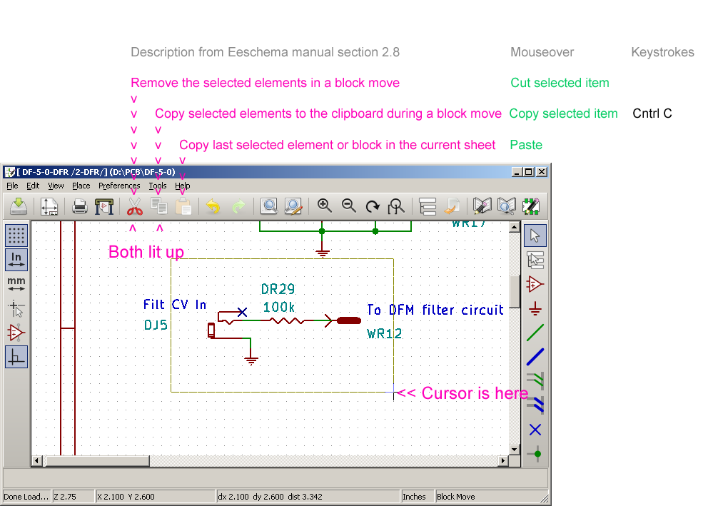
appear along the lines if the image below. The act of dragging, whether or not the
marquee selects any components, causes two buttons on the top toolbar
to light up, indicating that these buttons can be activated in the
current circumstances. The three top menu buttons we are
concerned with are most briefly identified by the first word of their
mouseovers: Cut, Copy and Paste (see image below). Note that the
mouseover terms for these three buttons do not appear in the manual,
nor does the keystroke command for the right menu item which appears to
have the same function as the Copy button: Control C. (These are
arguably bugs in the KiCad documentation.) We can't actually
access the Copy button with the mouse/trackball when we want it - we have to use Control C or
the right menu item mentioned below, which is called Save block (Cntrl+C). So why have a copy button if we can't press it?
- Assuming the marquee encloses one or more components, there are
four or five things which can be done now, all with the same effect.
Until one of these is done, or the block move (drag) operation (which
is what we initiate with the selection, and begin to activate by moving
the mouse/trackball after releasing the left button) is canceled by
the Esc key or a right menu item, then we cannot move the cursor
outside the Eeschema schematic editing area, nor use it to activate any
toolbar buttons or menu items.
- Without releasing the left button, press
Control C. The marquee disappears, the items are no longer
selected, the Cut and Copy buttons are dimmed and the Paste button
lights up.
- Release the left button, and do not move the
mouse/trackball. The selected components look weird, since the
image for them is partly reversed by the highlighting of selected
objects. Then press Control C. The selected items reappear
properly, the marquee disappears, the items are no longer selected, the
Cut and Copy buttons are dimmed and the Paste button lights up.
- Release the left button, and do not move the mouse/trackball. The
selected components look weird, since the image for them is partly
reversed by the highlighting of selected objects. Use the right click menu item: Save block (Cntrl+C). The selected items reappear properly, the marquee disappears, the
items are no longer selected, the Cut and Copy buttons are dimmed and
the Paste button lights up.
- As for b and c, except that the mouse/trackball is moved before
pressing Control C or using the right click menu item, which means we
see the original components and a copy of them ready to be placed by
the block move operation. The end result is the same, but before
the Control C or right click, the screen will display both the original
items and the set of copies of these items being readied for placement
by a block move (drag).
- Now the Cut and Copy buttons are dimmed and the Paste button is
lit up, indicating that there are one or more items in Eeschema's
"clipboard", for want of a better term:
If necessary, change to another sheet in the project, via the "Navigate schematic hierarchy" (mouseover text, AKA in the manual: "View and navigate the hierarchy tree").
Then, in the same or a newly selected sheet, click the brown clipboard icon on the top toolbar - the right one of these three, AKA the Paste button (according to its mouseover, but "Paste" this is not mentioned in the manual). This is the Paste operation - and the selected items (with '?' in their references) can be moved to their final resting place in the currently visible schematic, and placed wherever we like by pressing the left mouse/trackball button.
This Paste operation can be repeated many times, with the same "clipboard" contents, being placed in multiple places in the currently visible schematic. There seems to be no keyboard shortcut for the Paste button, we we have to use the mouse/trackball to click it, and then use the mouse/trackball to move the new copy wherever we want it.
According to: https://bugs.launchpad.net/kicad/+bug/1462193 this block select, copy to clipboard and paste operation only works between schematic sheets in different projects if Eeschema is opened independently, but not if Eeschema is run from the main KiCad program.
In all cases, whether we:
If the schematic, or the entire set of two or more hierarchical schematics in the whole project, has one or more components with question marks in their references like this, then it is not possible to generate a BoM. So we must sort these out and make proper references for all components by manual and/or automatic means, before proceeding to generating a BoM. A netlist can be generated from schematics in this state, but I have not investigated whether this would be desirable.
In all cases, whether we:
- Used the C key to make a copy of a single component into the current schematic sheet.
- We used the Control C and Paste button approach to make a copy of
a single component or a block of components and wires to the same
schematic sheet.
- We used the Control C and Paste button approach to make a copy of a single component or a block of components and wires to a different schematic sheet in the same project.
If the schematic, or the entire set of two or more hierarchical schematics in the whole project, has one or more components with question marks in their references like this, then it is not possible to generate a BoM. So we must sort these out and make proper references for all components by manual and/or automatic means, before proceeding to generating a BoM. A netlist can be generated from schematics in this state, but I have not investigated whether this would be desirable.
07 - The basic BoM CSV file
All the following is done with a
schematic design which is far from complete, with 4.0.7. The
supplied BoM creation program and translation file bom2csv.xsl is tricky to set up for Windows.
Please see the details at: ../#bomw - with its screenshot of what the results look like in a spreadsheet program.
This basic CSV BoM file contains a single line for each schematic component, where that single line covers a component with a particular reference, for its one or more sections. I generally assign references manually, but if I don't assign them, there will be a question mark, such as U? which will be changed to a suitable number by the automatic annotation system as part of the next netlist generation operation. It is only possible to generate a BoM once all components have their references fixed, manually or automatically.
A simple BoM like this is useful for checking all the fields of all the components, and this is quite an elaborate body of data which we need to get right.
For instance, a 4053 CMOS triple two-way multiplexer chip has a reference U4 for all three of its sections, and this leads to a single line in the BoM for what will be a single physical chip on the PCB.
Just by eyeballing the SN-xxx columns I can see that Mouser lists and presumably stocks all the more exotic components for which I have added stock numbers. If the prices were good, then a single order to Mouser would do the trick, depending on the freight costs of the other distributors. The T203-SHCQE switches are expensive and particularly hard to find in stock, so if they were significantly less expensive at OnlineComponents, it would make sense to order them and maybe some capacitors there, with a separate smaller Mouser order.
However, a BoM like this is not much use since it does not group, collate or whatever, multiple lines with the same part number into a single line with a quantity greater than one.
#group
08 - A BoM CSV file with grouping - and a bug fix for the original .xls file which produces these
The above mentioned basic BoM CSV file was created from an intermediate .XML netlist file written by Eeschema, and processed by the executable program xsltproc.exe (this is a Windows example) which is supplied as part of the KiCad 4.0.7 installation and which originates from http://www.xmlsoft.org/XSLT/ . The user manual is: http://www.xmlsoft.org/XSLT/xsltproc.html . This program uses a translation file, which is provided with KiCad: C:\Program
Files (x86)\KiCad\bin\scripting\plugins\bom2csv.xsl to transform data from the.XML file into the final .CSV file described above.
By modifying the translation file, it is possible to get a different kind of BoM result. Wolf Walter did this in September 2014:
I selected the text in the box of this forum post and copied it to a file bom2groupedCsv.xsl in the same directory as the original bom2csv.xsl file used above, and on which this is based:
Here is that file: the same text as from the above forum message, here with a .txt extension so it will not be treated in some weird way by your web browser. The name bom2groupedCsv.xsl is the name from Wolf Walter's forum message.
Special note:
Comparing the two (bom2csv.xsl and bom2groupedCsv.xsl) with Beyond Compare shows that only a handful of lines have been changed or added.
The incantation for creating a "plugin" for this (../bomw) , which I called XSLTPROC BOM-Grouped-Wolf-Walter-2014 is (it is all one line, and where you see a break from the first line on this web page to the second, you should have a space):
In Eeschema, once this has been entered into the dialogue box which arises from the BOM button on the top toolbar, and once I used the Generate button there, success was reported:
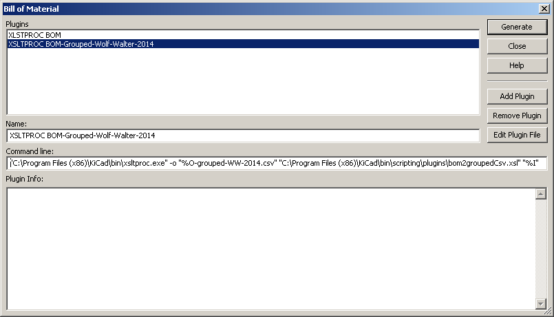
This is a success! This xlt language must be powerful, since only a few changed lines produce a different and much more usable result. There is one line per type of component, where type is the combination of the contents of the Value and Footprint fields. The lines are sorted by reference. The resulting file is a good way of checking that every component in the schematic which I want to be the same physical part has its fields set to achieve this.
However, not every such component which is grouped together to be represented by a single line will necessarily have all its other fields set the way I want them. I am not sure how this script chooses which component's fields to include in the line when two or more are grouped like this.
So a grouped BoM is no substitute for the simple ungrouped BoM mentioned in the previous section, for the purposes of checking the details of all the fields in all the components.
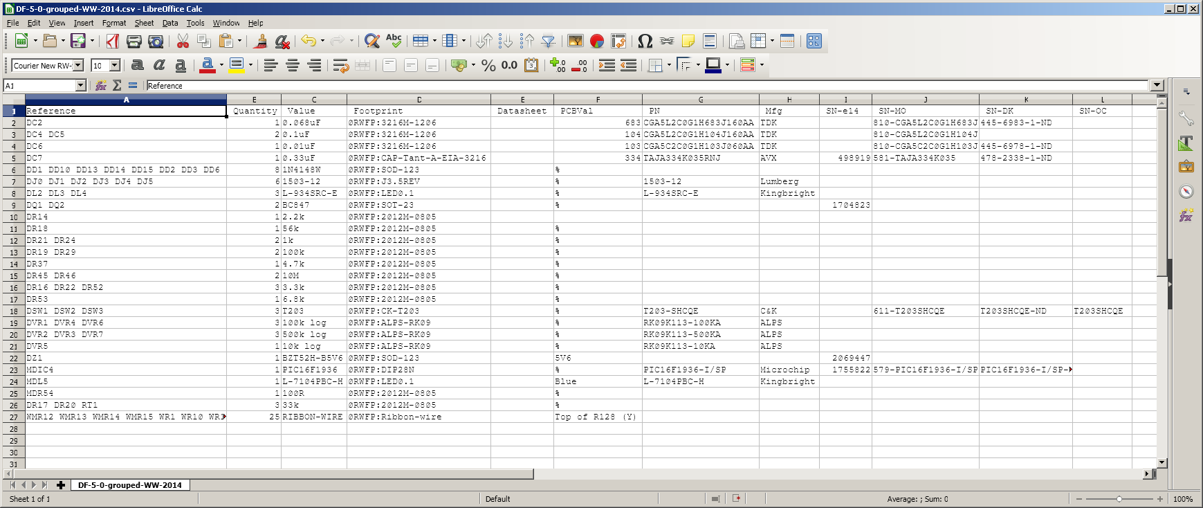
Here is what the resulting BoM (project-name-grouped-WW-2014.csv) looks like in a spreadsheet program:
The conversion script bom2grouped_csv.xsl which is included in KiCad 4.0.7 produces similar results, but there are problems with its output, at least with my particular schematic. Its .CSV file contains lots of things in double quotes. I assume this is an attempt to avoid any characters in component fields which would be interpreted as delimiters in a .CSV file being interpreted as such by whatever spreadsheet or other program reads the .CSV file.
I think bom2grouped_csv.xsl was added to KiCad on 2016-06-03 (see log entry: https://git.launchpad.net/kicad/commit/?id=93e61e7a2e963f956d05299c72b403ae3eccb110 and here).
I have been unable to trace the origin of this file, but it was added by Jean-Pierre Charras who attributed it: "(from a contributor)". It may be a derivative of another file which can be found in these locations:
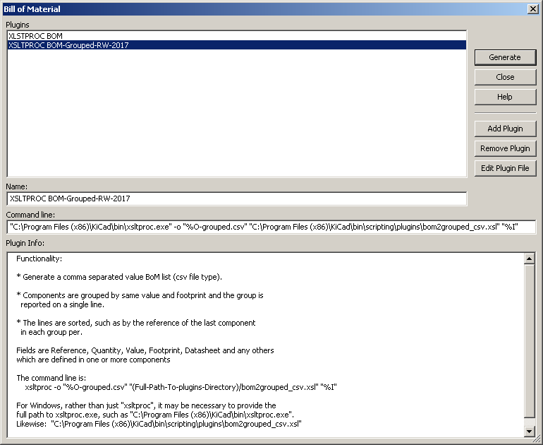
Here is my incantation to make it work as a plugin named XSLTPROC BOM-Grouped-JPC-2016:
Here is what the Bill of Material dialogue box looks like after I pressed the Generate button:
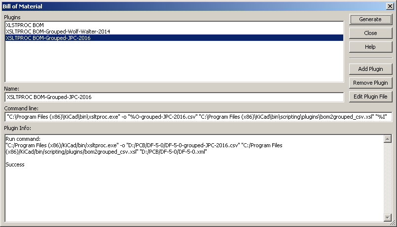
When the resulting BoM file:
is read by Libre Office Calc 5.4.2.2, some problems are apparent:
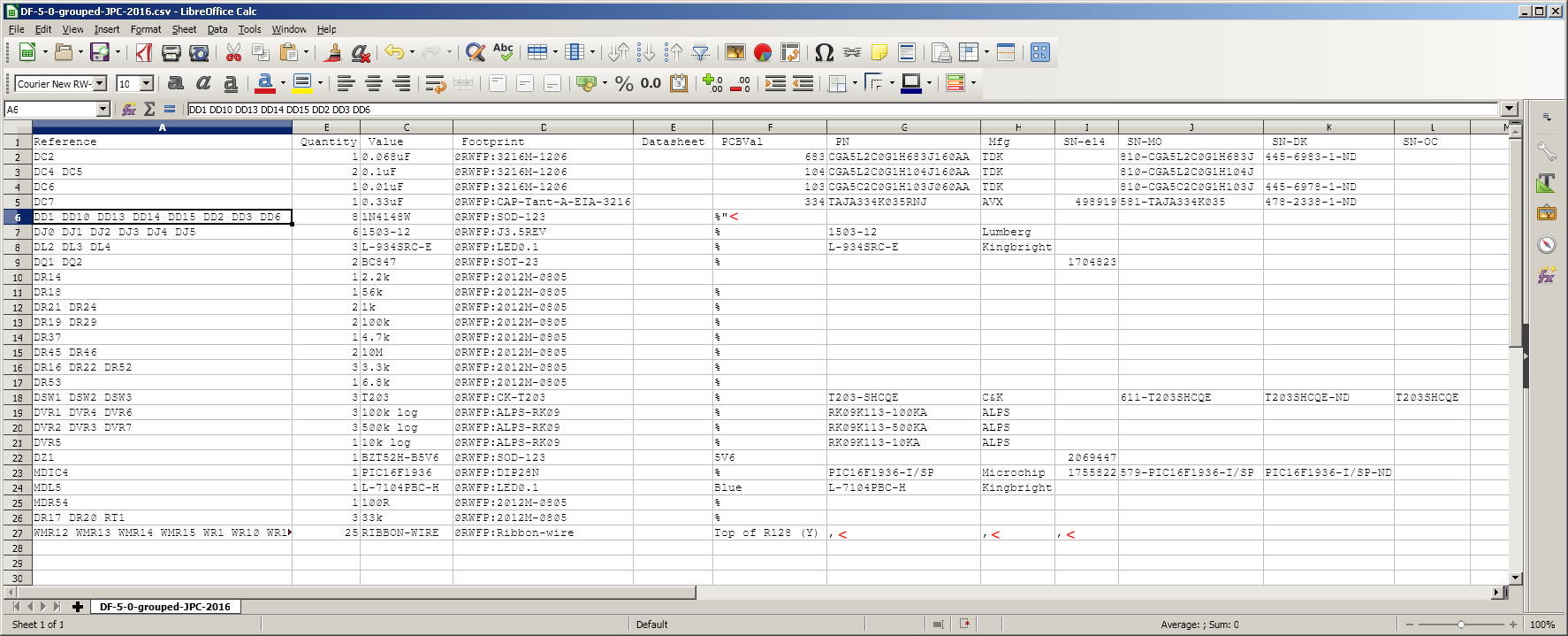
Reading it with Excel 2003 produces the same errors, except that there is a space between the % character and the double quote character on line 6.
Neither of these two conversion files are satisfactory, though the first one works for me so far.
I reported this as a bug: https://bugs.launchpad.net/kicad/+bug/1722138
I have no idea how this xlt conversion language works, but I produced a version of the current bom2grouped_csv.xsl file which fixes the problems exemplified in the above screenshot. This version also improves the indenting of the text of the .xsl program itself and has improved documentation of what it does and how to use it, which is made visible to the use in the BoM generation dialogue box.
Here is the new version bom2grouped_csv-RW-2016.xsl.txt . I intend that you download it, rename it to bom2grouped_csv.xsl and copy it to wherever that file was, in your Windows, Linux or Mac system. For my installation, I put it at:
Then I created a plugin to use it, with the BOM button's dialogue box: Add Plugin. I selected the program to run, as noted above, which is:
named the plugin "XSLTPROC BOM-Grouped-RW-2017" and altered the command line to:
Once this plugin is selected, it documents its functionality and how to construct the command line:
The resulting BoM file:
has no such quoting problems and works fine with Libre Office Calc, Beyond Compare and Excel 2003:
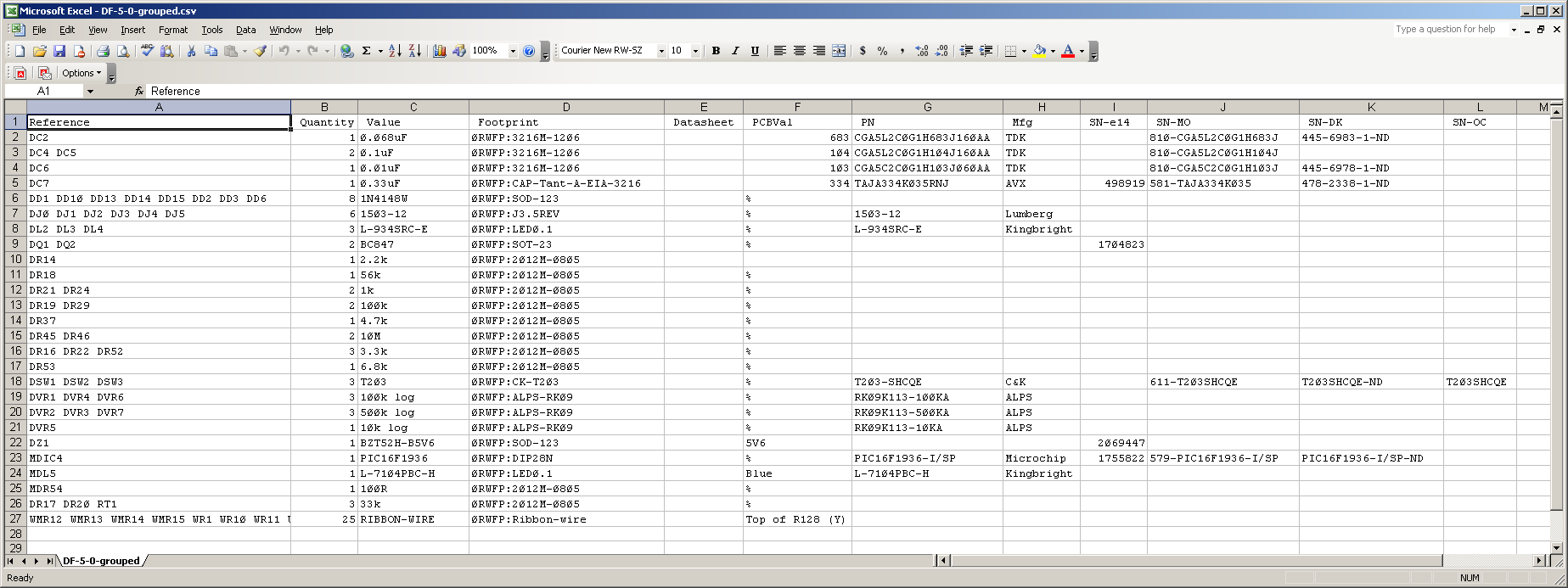
This is good enough for me to work with for now. However, I also explored a more powerful, flexible and better-documented Python approach to making BoMs: ../kicad-python-bom-scripts/ .
By modifying the translation file, it is possible to get a different kind of BoM result. Wolf Walter did this in September 2014:
I selected the text in the box of this forum post and copied it to a file bom2groupedCsv.xsl in the same directory as the original bom2csv.xsl file used above, and on which this is based:
C:\Program Files (x86)\KiCad\bin\scripting\plugins\
Here is that file: the same text as from the above forum message, here with a .txt extension so it will not be treated in some weird way by your web browser. The name bom2groupedCsv.xsl is the name from Wolf Walter's forum message.
Special note:
This file is not to be confused with a file bom2grouped_csv.xsl which is included in the C:\Program Files (x86)\KiCad\bin\scripting\plugins\
directory with KiCad 4.0.7. This later file (with the underscore
and lowercase c)
has some additional changes to place many data items from component
fields in double quotes, so that any commas or similar characters in
those data items are not interpreted as cell delimiter characters by
whatever programs read the .CSV file. However, there are bugs in this. See below for details and a fix.
Comparing the two (bom2csv.xsl and bom2groupedCsv.xsl) with Beyond Compare shows that only a handful of lines have been changed or added.
The incantation for creating a "plugin" for this (../bomw) , which I called XSLTPROC BOM-Grouped-Wolf-Walter-2014 is (it is all one line, and where you see a break from the first line on this web page to the second, you should have a space):
"C:\Program
Files (x86)\KiCad\bin\xsltproc.exe" -o "%O-grouped-WW-2014.csv" "C:\Program
Files (x86)\KiCad\bin\scripting\plugins\bom2groupedCsv.xsl" "%I"
In Eeschema, once this has been entered into the dialogue box which arises from the BOM button on the top toolbar, and once I used the Generate button there, success was reported:
This is a success! This xlt language must be powerful, since only a few changed lines produce a different and much more usable result. There is one line per type of component, where type is the combination of the contents of the Value and Footprint fields. The lines are sorted by reference. The resulting file is a good way of checking that every component in the schematic which I want to be the same physical part has its fields set to achieve this.
However, not every such component which is grouped together to be represented by a single line will necessarily have all its other fields set the way I want them. I am not sure how this script chooses which component's fields to include in the line when two or more are grouped like this.
So a grouped BoM is no substitute for the simple ungrouped BoM mentioned in the previous section, for the purposes of checking the details of all the fields in all the components.
Here is what the resulting BoM (project-name-grouped-WW-2014.csv) looks like in a spreadsheet program:
The conversion script bom2grouped_csv.xsl which is included in KiCad 4.0.7 produces similar results, but there are problems with its output, at least with my particular schematic. Its .CSV file contains lots of things in double quotes. I assume this is an attempt to avoid any characters in component fields which would be interpreted as delimiters in a .CSV file being interpreted as such by whatever spreadsheet or other program reads the .CSV file.
I think bom2grouped_csv.xsl was added to KiCad on 2016-06-03 (see log entry: https://git.launchpad.net/kicad/commit/?id=93e61e7a2e963f956d05299c72b403ae3eccb110 and here).
I have been unable to trace the origin of this file, but it was added by Jean-Pierre Charras who attributed it: "(from a contributor)". It may be a derivative of another file which can be found in these locations:
https://github.com/ContextualElectronics/KiCad-BOM/blob/master/bom2groupedCsv.xsl (ChrisGammel)
https://github.com/jim17/memtype/blob/master/schematic_pcb/bom2groupedcsv.xsl (Noel Carriquí Ojeda oyzzo)
https://github.com/jim17/memtype/blob/master/schematic_pcb/bom2groupedcsv.xsl (Noel Carriquí Ojeda oyzzo)
Here is my incantation to make it work as a plugin named XSLTPROC BOM-Grouped-JPC-2016:
"C:\Program
Files (x86)\KiCad\bin\xsltproc.exe" -o "%O-grouped-JPC-2016.csv"
"C:\Program Files
(x86)\KiCad\bin\scripting\plugins\bom2grouped_csv.xsl" "%I"
Here is what the Bill of Material dialogue box looks like after I pressed the Generate button:
When the resulting BoM file:
is read by Libre Office Calc 5.4.2.2, some problems are apparent:
Reading it with Excel 2003 produces the same errors, except that there is a space between the % character and the double quote character on line 6.
Neither of these two conversion files are satisfactory, though the first one works for me so far.
1 - The older file bom2groupedCsv.xsl
(which Wolf Walters posted to the forum in 2014, and is not included as part of KiCad) does
not have all the fancy double quoting arrangements of the later file,
and so can be expected to produce erroneous results if any of the
fields contain characters which a .CSV reading program considered to be
delimiter characters.
2 - The newer file bom2grouped_csv.xsl, which is part of the KiCad distribution, produces obvious errors with my very small schematic. Furthermore, its results completely confused Beyond Compare which interpreted one line in such a way that the newline was not recognised.
2 - The newer file bom2grouped_csv.xsl, which is part of the KiCad distribution, produces obvious errors with my very small schematic. Furthermore, its results completely confused Beyond Compare which interpreted one line in such a way that the newline was not recognised.
I reported this as a bug: https://bugs.launchpad.net/kicad/+bug/1722138
I have no idea how this xlt conversion language works, but I produced a version of the current bom2grouped_csv.xsl file which fixes the problems exemplified in the above screenshot. This version also improves the indenting of the text of the .xsl program itself and has improved documentation of what it does and how to use it, which is made visible to the use in the BoM generation dialogue box.
Here is the new version bom2grouped_csv-RW-2016.xsl.txt . I intend that you download it, rename it to bom2grouped_csv.xsl and copy it to wherever that file was, in your Windows, Linux or Mac system. For my installation, I put it at:
C:\Program Files (x86)\KiCad\bin\scripting\plugins\bom2grouped_csv.xsl
Then I created a plugin to use it, with the BOM button's dialogue box: Add Plugin. I selected the program to run, as noted above, which is:
C:\Program Files (x86)\KiCad\bin\xsltproc.exe
named the plugin "XSLTPROC BOM-Grouped-RW-2017" and altered the command line to:
"C:\Program
Files (x86)\KiCad\bin\xsltproc.exe" -o "%O-grouped.csv" "C:\Program
Files (x86)\KiCad\bin\scripting\plugins\bom2grouped_csv.xsl" "%I"
Once this plugin is selected, it documents its functionality and how to construct the command line:
The resulting BoM file:
has no such quoting problems and works fine with Libre Office Calc, Beyond Compare and Excel 2003:
This is good enough for me to work with for now. However, I also explored a more powerful, flexible and better-documented Python approach to making BoMs: ../kicad-python-bom-scripts/ .
#other
09 - Other approaches to generating BoMs
There is a Pascal (!) program with source and Windows executable:
Im 2016 I tried release 1.01 from June 2015 with 8.0.2-stable. It is a GUI application into which each schematic file must be read manually. It builds up a simple BoM and grouped BoM in the tabbed windows, and enables the result to be written to a CSV file. It did not, in my experience, pick up data in the fields I have added to the system as described above.
See also may page looking at a fancy Python approach to generating KiCad BOMs: ../kicad-python-bom-scripts/
Update history:
- 2016-04-27: Initial version.
- 2016-04-28: Revised in light of kicad-pcb-value now using the first character of the PCBVal field being '%' or not to determine whether or not to make a change. So we no longer need to rename the PCBVal field to PCBVal- in order to inactivate it.
- 2017-10-08 Revised for KiCad 4.0.7, to mention Python approaches to making BoMs, and to report on the fixed version of bom2grouped_csv.xsl which does not seem to have quoting problems.