A
potentially novel "Op-Amp Follows FET" pre-amplifier for electret
microphones which have separate connections for the internal FET's
Source and Drain: lower distortion and higher sound levels
|
Robin Whittle rw@firstpr.com.au 2009-09-26
<<< To the parent page where there is a link
to a page which depicts the dismantling of several various Transound
microphones,
including a TSB-140AO 14 mm omni capsule which I am using for these
experiments. That page also links to the Micbuilders discussion
list.
Summary:
I present a potentially novel "Op-Amp-
Follows FET" pre-amp for condenser microphones which have an internal
FET with both its Drain and Source available as separate connections.
Please let me know if you have seen this sort of design before.
This pre-amp enables the capsule to be used at significantly
higher sound levels than is possible with the two conventional methods
of biasing electret capsules with internal FETs.
The resulting performance does not equal that of a properly designed
externally polarized condenser microphone. Such a microphone can have a
large gap between the diaphragm and backplate and still be reasonably
sensitive due to the high voltage externally applied.
There are
bound to be physical limits on the sound levels electret capsules can
handle, no matter what electronics is used with them. In order to
be reasonably sensitive, with their built-in elecret polarization which
is presumably less than the voltage applied to externally polarized
condenser microphones, they would tend to have a smaller gap between
the diaphragm and backplate. For a given cavity depth (in an omni capsule), this means
the electret capsule will distort at sound levels below those at which
an otherwise similar externally polarized capsule would distort.
Nonetheless, there are applications where it is desirable or essential to get better
performance from electret microphones. Electret capsules have
advantages over externally polarized condenser mics, including:
- Electrets and their support electronics are much less expensive.
- Electrets and their support electronics require less power, are more compact, are simpler and are therefore much more reliable.
- As
far as I know, electret condenser microphones are far less
affected by humidity in terms of there being spikes in the output than
externally polarized condenser microphones. (However, in the long
term, an electret mic may loose sensitivity if humidity affects its
electret's charge - while an externally polarized condenser microphone
has no such charge to lose.)
This is a first attempt, not at all a definitive work. I have
only tried the new circuit on one particular microphone. The results are
promising: much higher sound levels without DC bias change problems
("DC Thump") and, at high SPLs, lower distortion than with the usual
ways of biasing these microphones.
There remains a limitation, which is probably inherent to the capsule I
tested, rather than the pre-amp, of gain reduction at sound levels of
135 and 140 dB SPL or more. I think this would be barely perceptible at
135 dB SPL, and perhaps would be barely perceptible at 140 dB
SPL. However, it is a limitation.
When using the best conventional technique (Source Follower) there are
problems with "DC thump" and distortion which limit the quality of the
microphone's response much above its rated maximum of 120 dB SPL.
So, within some limitations, it is possible that the new pre-amp
extends the high SPL limit for this capsule by about 20 dB.
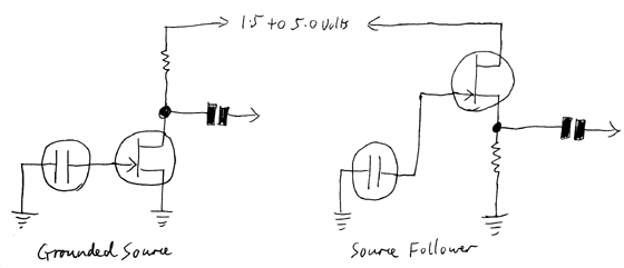
I analyze the two common ways of biasing such microphones:
- Grounded Source
with pull-up resistor from the Drain - as is used
for pretty much all two-terminal electret mics. This gives high
sensitivity but limited high SPL response, due to distortion and "DC
thump" at the onset of high SPLs. "DC thump" means that the
average voltage of the audio output changes appreciably with the onset
of the loud sound - and changes back again when the sound signal
returns to lower levels. Nonetheless, this is a simple,
high-gain, arrangement which is probably quite suitable for modest
sound levels. This system produces a negative signal for an
increase in sound pressure, while Source Follower and the new pre-amp
produce a positive signal.
- Source Follower
- the circuit which is recommended for the
TSB-140AO: the Drain is connected to a positive DC voltage and the
Source drives a load resistor to ground. This has lower gain than
the Grounded Source system, but still suffers from DC thump above about
120 dB SPL, and
has higher levels of distortion than the new pre-amp.
The new (as far as I know) "Op-Amp Follows FET" circuit runs the FET at a constant current and
with constant relative voltages between Gate, Source and Drain.
The Gate is connected directly to the backplate voltage and the op-amp drives the whole
circuit surround the FET up and down to follow the backplate voltage exactly.
The sensitivities I measured with the three approaches are as
follows. The differences are significant. The absolute
values of the sensitivities are uncertain because I don't know how
accurate my reference sound level meter is. The test signal was
114 dB SPL 1 kHz.
Method mV RMS @ 1 pascal Relative to 1 V RMS per
= 94 dB SPL pascal
Grounded Source
6.8k 2.5V 35
mV
-27 dB
4.9V 39
mV
-26 dB
Source Follower
6.8k 1.5V * 7.4
mV
-40 dB
4.9V 7.6
mV
-40 dB
New pre-amp 7.4
mV
-40 dB
*
Specification
-45 +/- 4 dB
This circuit might also be of interest to people making pre-amps for
electret and externally polarized condenser microphones which have no
internal FET. (If a single FET's noise is the limiting factor, perhaps two or four could be run in parallel.)
Some "two terminal" electret microphones can be modified to provide
separate access to the Source and Drain of the internal FET.
This, together with a new arrangement for biasing the modified
capsule,
is known as the "Linkwitz modification" (Linkwitz mod) and was first
developed, or at least first made widely known, by
Siegfried
Linkwitz:
So perhaps this new pre-amp circuit could be applied to electret capsules modified in this way.
This is a preliminary page - I intend to do more thorough design and
testing in the future and will link to the resulting web page from here.
The test arrangements are not necessarily very accurate in terms of
absolute sound levels - I was using a cheap sound meter. I guess
they are accurate within a few dB SPL. The tests were purely of
1kHz at sound levels between 110 dB SPL and 140 dB SPL. I
have not yet measured frequency response or background
noise. Nor have I yet done any listening
tests.
The TSB-140AO
Please see the parent page for another page with more details. Here are the key points.
This is a Transound omni electret microphone with an internal FET. The datasheet is:
I bought this and other Transound microphones from
JLI Electronics in the USA:
These are the omni version of the "unidirectional" TSB-140A.
They are 14mm in diameter. They are a "back electret" design with
a layer of charged fluoropolymer (I assume) on the front of the
backplate.
The diaphragm is 3 um thick aluminized mylar (I assume) with the aluminization layer, which is grounded, on the front.
The back of the diaphragm is non-conductive, but capacitively
coupled, by 3 um of mylar, to the grounded front of the diaphragm.
The
effective diameter of the diaphragm is 10.5mm.
Between the diaphragm and backplate, the
spacer ring is ~60 um thick.
Behind the backplate is a
sealed cavity with an effective depth of about 0.7 mm.
The backplate connects directly to the gate of an N-channel FET, which is the "J34" grade of
2SK1109:
2SK1109-datasheet.pdf
I think the datasheet for the FET is somewhat misleading - see the next section.
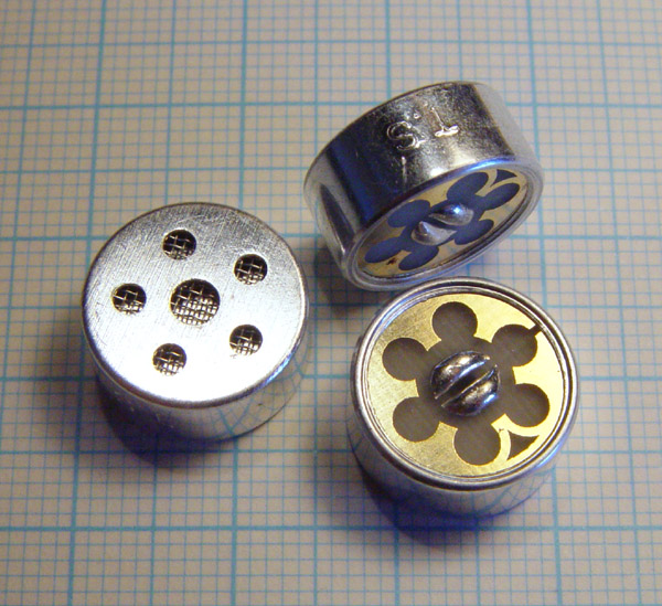
At the back we have Ground, Source and Drain. For the capsule at
the lower right of the above photo, the Ground is the gold-plated
tracks, the Drain is to the upper left and the Source is to the lower
right.
Scrutinizing the 2SK1109 N-Channel FET
The only access to the backplate we
have is through the gate of the FET - so we have to do
everything via the FET's Source and Drain. We need to get to
know this device as well as possible.
Please take a good look at the datasheet:
This does not appear to be one of the FETs in current production at
NEC. The current ones have rather similar specifications.
Maybe this pre-amp design will work just as well with FETs other than
the 2SK1109. (Thanks to
Richard Crowley
of the Micbuilders list who told me that the FET's only markings - "J34" - mean it is probably a 2SK1109.)
The current production NEC FETs are all for Electret Condenser Microphones (ECMs):
I guess that Transound use the 2SK1109 in this particular capsule because
its package has long pins which are amenable to the Source and Drain being soldered to the
PCB, with the Gate pin being bent over and pressed against the
gold-plated stud. I guess they bought a bunch of them, or that
NEC still makes them without having them for sale to other
companies. I don't think any of the current production NEC FETs
have this package.
As far as I can tell, the "EQUIVALENT CIRCUIT" is quite misleading. Starting at the left . . .
The left diode, from Gate to Source,
does exist as a natural part of any N-channel J-FET. However, the
same is true of Gate to Drain as well, and no such diode is shown. This diode behavior has
quite a high resistance.
The right diode does appear to exist -
cathode to Gate and anode to Source. However, perhaps it is not exactly
as shown, since it is possible (according to the datasheet's "Gate
Cut-off Voltage" spec) to have the Gate 1.0 volts negative with respect
to the Source.
There appears to be, in effect, a higher resistance diode with its cathode to the Drain and its anode to the Source.
The resistor does not exist in such a
simple form as the diagram shows. The datasheet gives no
information about it whatsoever, but datasheets of other FETs refer to
it as having a purpose of quickly stabilizing the Gate voltage to
whatever voltage is desired.
I think this "resistor" is more likely leakage between the Gate to various parts of the channel between the Source and Drain.
If there were no diodes or "resistor" connecting to the Gate, there
would need to be some external component, such as a resistor of
hundreds of megohms or a giga-ohm, to stabilize the backplate and
therefore the Gate voltage somewhere desirable, such as between the
Source and Drain voltages or maybe a few hundred mV below the Source
voltage.
I can't be sure, but I think it is best to think of the "resistor"
causing the Gate voltage to stabilize, on average, at some voltage
between the Source and Drain voltages.
In the two conventional methods of driving these capsules, with high
SPLs there is wide variation in the Source voltage or the Drain
voltage. Either way, the Drain-Source voltage varies with the
sound signal and I believe this leads to current flowing into and out
of the capacitance of the backplate-diaphragm capacitor. As far as I know,
this is the cause of the "DC thump".
A key feature of the new pre-amp circuit is that the Source to Drain
voltage and current remains constant. Also, the Gate voltage with
respect to Source and Drain remains constant. Therefore, no
matter what audio signals are encountered (as long as they are within
the tracking range of the op-amp) from the FET's point of view, nothing
changes. Therefore, the Gate voltage, with respect to the Source
and Drain, will stabilize. No matter what sound signal, there is
no overall current flowing in or out of the Gate. Therefore,
there is nothing to charge up or discharge the backplate-diaphragm
capacitance. So the new circuit does not have a problem with "DC
thump" at high SPLs.
I think these FETs are designed for cheap, mass-market, small, electret
microphones. In those microphones - of which surely a billion or
more are made each year, primarily for cellphones - the Source is grounded, and
the Drain is pulled up by a load resistor to some low voltage such as
1.5 or 3 volts.
It is this "Grounded Source" mode which I think the datasheet is
intended to be relevant to. The noise test diagram uses this mode.
The "Forward Transfer Admittance" in micro siemens appears to be the
slope of the curves on page 5, with the Drain to Source voltage being
about 5 volts.
The FETs are sorted into several "Ranks". I think of these as
"grades". The one used in the Transound capsules I bought were
the "J34" rank - those with a Source to Drain current between 90 and
180 uA, when the Drain is +5.0 V above the Source, and when the Gate is
the same voltage as the Source.
In actual usage, with the Gate connected only to the backplate, I doubt
that such a condition would persist for long, since it is my impression
that leakage, the "resistor" or whatever would charge the Gate up to
some positive voltage, such as several volts with respect to the Source
if the Drain was as much as 5 volts positive with respect to the Source.
Anyway, this "Zero Gate Voltage Drain Cut-off Current" spec of 90 to
180 uA seems to be important for the Grounded Source mode.
There are no figures in the FET's datasheet to tell me what I most
wanted to know: the relationship between Gate voltage (with respect to
the Source) and Source-Drain current, when the Source - Drain voltage
was relatively low, such as 0.0 to 0.4 volts. I could infer
something from the far left side of the charts on page 4: that for zero
Gate to Source voltage, the Source to Drain connection would behave
like a resistor for Source Drain voltages of up to about 0.2 or maybe 0.3
volts. Above that, the FET's channel starts pinching off not so much at
the Source, but at the Drain, where the difference between the channel
voltage and the Gate voltage is higher - leading to a thinner channel
in that area.
In the future I plan to point to some diagrams regarding pinch-off of
J-FETs - but first I want to be sure I understand what is occurring,
since I doubt that all the diagrams on the Net are entirely accurate.
To fully understand what actually happens in Grounded Source and Source
Follower mode, one would have to look very carefully at the innards of
the FET, and in particular how its channel pinches off more at the
Drain (or whichever of Drain and Source is more positive) and how the
voltage of the channel at various parts between Drain and Source will
therefore lead to more or less constriction of the channel. The open part of
the channel forms a resistor, and I think this channel can become quite a narrow
near the Drain, assuming the Drain is significantly more
positive than the Source.
For the new circuit, we can ignore a lot of these things. All we
require of the FET is that its leakage, or resistance, or whatever,
tends to stabilize the Gate voltage, with respect to the Source and
Drain, at some stable level provided we keep the Source Drain voltage
fixed. In this circuit, I intended to keep this voltage to about
0.2 to 0.3
volts - within or at the edge of the resistive regime. In fact,
the FET runs at about 0.277 volts, which according to the datasheet is
at the start of the pinch-off regime. Still, it seems to work
fine.
At that Gate voltage, we have a certain resistance between
the Source and Drain. Raising the Gate voltage with respect to
the other two will increase the current in the FET because the gate
will no longer narrow the channel so much. Lowering the Gate
voltage with respect
to the other two will cause the resistance to increase - and so cause
the Source to Drain current to fall. (I am speaking loosely of
electron current.)
In this low-voltage, fixed voltage, mode of operation, it is probably
best to think of the Gate being loosely resistively coupled, via very
high value resistors which are really leakage currents to various parts
of the Source - Drain channel, which are themselves at a range of
voltages between that of the Source and the Drain.
In the new circuit, the Gate stabilizes to some voltage which maintains
the current, which in our circuit gives rise to the Source to Drain
voltage. It doesn't matter whether this Gate voltage is at, or a
little below the Source voltage, or anywhere up to the Drain voltage or
a little beyond. All that matters is that it is some voltage
between the two, and that at this voltage, no current flows in or out
of the Gate terminal.
For production, it would be necessary to find FETs with characteristics
at both extremes of the allowed range and ensure the circuit would work
equally well with the full range of FET behavior.
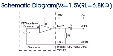
The Op-Amp Follows FET circuit
Here is a schematic - just a rough hand-drawing:
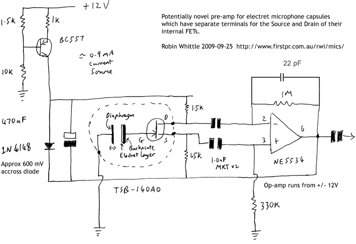
I spent several days trying to devise a circuit by which the Source and
Drain would be driven up and down to follow the Gate voltage. I
tried a single load resistor and sensing either the Source or Drain
voltage, but could not produce a stable circuit.
This design worked first time and these are my original component
values. A properly optimized design would no-doubt be
different. For instance, the 1 M resistor should probably be 330
k.
The current source, diode and capacitor maintains 0.59 to 0.6 volts
across the electrolytic capacitor, no matter how the op-amp drives the
negative terminal of the capacitor (at least within a +/- 10 volt range
of ground). The 470uF value is over-engineered, probably a
smaller value would do. There could also be a negative current
source with the same 0.9 mA current, pulling down on the cathode of the
diode - so the op-amp only needs to drive the 0.6 volt supply circuit
up and down with a very light current. If the voltage excursions
were not too great with respect to the positive supply voltage, it might be possible to replace the current source with a resistor.
I chose the 1.5 k resistors to match what I though was the resistance
of
the FET when its Gate terminal floats to the point of no more leakage
and when the Drain to Source voltage is about 0.2 volts.
At that voltage, the FET would be working within its resistive range,
before the pinch-off
effect at higher Drain voltages causes the current to be pretty much
limited, no matter how high the Drain voltage rises above the Source
voltage. According to the graph below, the FET is operating just
where the resistive regime gives way to the pinch-off regime.
There "0.6 volt" supply is 0.595 V.
The Source to Drain current is 106 uA.
The voltage across each 1.5 k resistor is 0.159 V. So the Source to Drain voltage is 0.277 V. From the
data sheet, for the J34 rank:
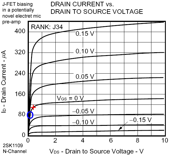
I think the FET is operating somewhere between the blue
O region and the red
+ region. The design goals are:
- Minimise the voltage across the FET, which I intend will cause the Gate leakage current is relatively minimal and stable.
- Use a relatively low voltage, such as 0.6 volts for the local
power supply for the FET, so this voltage and the current source does
not overly impede the capacity of the op-amp to push the whole circuit
up to nearly the positive supply rail.
- Maximise the relative voltage change between Source and Drain for
an infinitesimal rise in Gate voltage relative to these to
voltages. This is to maximise the "error" signal which the op-amp
amplifies in order to make the whole circuit track the changes in Gate
voltage.
Goals 1 and 2 seem to be achieved OK with this 0.277 volt arrangement,
though a lower voltage such as 0.2 volts would probably be fine too.
The aims of goal 3 are compromised as the bias point moves down the resistive slope, starting somewhere between
+ and
O.
As it is, the FET is biased around the top of that slope, which looks
good. Goal 3 should still be achieved with higher voltages across
the FET, but this would compromise goals 1 and 2.
For this particular FET, I think these resistors are a good
value. About half the voltage drop is in the resistors and the
remainder is in the FET.
I haven't yet measured the Gate voltage with respect to the Source and
Drain. That could only be done with a FET from a dismantled
capsule. The measurement could be by letting the Gate charge a
small capacitor, and then measuring its voltage with a FET or MOSFET
input op-amp - or by forcing the Gate to a known voltage which gave the same
current with these resistors.
AC changes in the Source to Drain voltage are coupled directly to the
op-amp's input, via the two 1.0 uF capacitors. In AC terms, the op-amp instantly drives the whole 0.6
volt supply circuit and its FET up or down as required to maintain the same Gate
to Source and Gate to Drain voltage.
My choice of 1 M and 330 k resistors was just a first guess. In
principle, these centre the output of the op-amp around 0 volts.
Because of input bias currents in the op-amp, and probably offset
voltages and offset currents, and due to the different resistor values,
my initial test circuit stabilises with the op-amp output at about 0.31
volts. More careful design could reduce this offset voltage, although this 0.3 volts presents no problems whatsoever.
Careful choice of capacitor and resistor values should enable the
circuit to respond to very low frequencies, including infra-sound
signals of interest to vulcanologists.
Without the 22 pF capacitor, the circuit oscillated at some RF
frequency. More careful design work would probably result in a
different value or some other way of stabilising the circuit without
upsetting high frequency response. I doubt this 22 pF would
attenuate frequencies below 20 kHz, since it is working into an
approximately (1.5 / 2) k ohm input impedance. Still, it would be
good to keep the response high for ultrasound purposes.
I have not tested the circuit for noise.
Noise would arise from at least these sources:
- Random impact of air molecules on the diaphragm. This
moves the diaphragm according to its mass and how it is damped -
stretched across its metal holding ring and
also by the pressure of air in the internal cavity. This creates
electrical noise in proportion to how sensitive the microphone is,
which is primarily a function of the effective electret voltage, the
gap between the diaphragm and the front of the back-plate, but also
other things such as capacitance of the back-plate to ground.
- Inherent electrical noise due to the resistive impedance of the
backplate with respect to ground, via the capacitance of the backplate-diaphragm gap. I assume this would be a very
low resistance of a few ohms or less, and would not be significant.
- Voltage noise in the Gate of the FET, and any other noise in the
current which flows though the Source to Drain channel. Some of
this noise would be inherent to the resulting resistance of the
FET's channel.
- Noise in the leakage current inside the FET to the Gate, and in
any other leakage currents to the Gate or backplate. I am
assuming that these, once applied to the capacitance of the backplate-diaphragm system,
would result in a voltage which is low enough not to worry about.
- The noise inherent in the resistance of the 1.5 k resistors, as
connected to the Drain to Source resistance.
- The current noise of the op-amp, as imposed on the resistance or at least AC impedance
of the the FET and its two 1.5 k resistors with respect to the output
of the op-amp. These 1.5 k resistors are nice low values and I recall that bipolar op-amps such as the one I used - the
NE5534 - work well with such low source impedances.
It is possible that the FET's voltage noise on its Gate would exceed,
or add significantly, to the inherent physical self noise (point 1
above) of the capsule. I suspect not, but I haven't tested it
yet. Assuming this is not the case, I would think that the
low-impedance drive to the low-noise bipolar op-amp should result in
minimal additional noise.
Later, I will refine the design with more experimentation, a proper
CCIR 468-4 noise measuring system (I intend to write my own software
for this) and with the latest low-noise bipolar op-amps, such as the
LME49710 or the dual
LM4562 .
Electrically, the circuit seems to behave well - it seems to track the
backplate voltage without any fuss. In practice - at least with
the particular TSB-140AO cartridge I tested - there were limitations at
high SPLs. These limitations became significant before the op-amp
started hitting its limits near the +/- 12 volt power rails - and as
far as I know, the limitations were occurring inside the capsule
itself, not in the FET or the pre-amp itself.
The only limitation I encountered in my test was a reduced gain at very
high SPLs, such as 135 and 140 dB SPL. I think this could not
occur in the electronics, since the exact FET current and 1.5 k
resistor values do not alter the gain of the circuit, which is
precisely 1.0 with respect to the Gate voltage. The gain dropped
over a period of seconds with 1 kHz at these very high SPLs, and then
restored itself in the seconds after the sound stopped. More on
this below, after an explanation of the test setup and the conventional
approaches to biasing electret capsules.
The prototype circuit is located directly at the rear of the capsule. I have not tried to shield it from interference.
If it were desired to mount the pre-amp somewhere other than directly
at the capsule, then some care would be required with shielded
cables. There would surely need to be two shielded cables to the
Source and Drain pins, but the shield of the Source cable should be
connected not to ground but to the bottom of the Source's 1.5 k load
resistor - the output of the op-amp. Probably the same would be
true for the shield of the Drain cable, but perhaps that should be
connected to the top of the Drain's 1.5 k load resistor.
There may be a way of making this work with shielded cables longer than
a few tens of centimetres - I haven't thought about it in detail
yet.
I think the ideal solution would be to mount the pre-amp right at the
capsule, and so take +/- 12 volts, or a little less, to that
location. The pre-amp's output would be extremely low impedance,
and with a resistor such as 100 ohms or so, to avoid too much
capacitive loading, I expect it would drive a long shielded
cable.
It might be desirable to use a dual op-amp so a phase inverter can be
included, so providing balanced outputs. Then, with some care and
a local regulator, it may be possible to run the entire pre-amp from a
positive supply, let the local regulator fix the centre-rail, connect
the case of the capsule to the centre-rail, and use the balanced
outputs and a differential receiver at the other end of the cable to
handle any noise in the locally produced centre-rail. Probably an
entire phantom power system could be integrated into the pre-amp
assembly.
The test setup
The test set-up was optimized for
convenience. I plan a much better arrangement in the future,
starting with a measurement microphone, such as the
Josephson C550.
I created a 48 kHz sample rate .WAV file with 1kHz to a level about 3dB
below clipping, and recorded this to a DAT. The DAT drove a
Yamaha DA202, which uses double-oversampling (or is it quad
oversampling?) with PCM53P 16 bit converters. This signal went
into a hi-fi amp of no special pedigree and into a midrange driver with
a considerable pedigree.
This was an ATC 3 inch soft-dome midrange driver, one of two I bought,
with matching 1.5" Audax soft-dome tweeters, in the early 1980s.
They were spares for ATC SCM-150 loudspeakers, pictured
here in some kind of audio shrine. One mid-range driver closely resembles the legendary
SM75-150S and the other one is similar, but has a bigger magnet and is 16 ohms. I used this second one for the tests.
The face of the driver was closed off with some reasonably rigid
material to form a small cavity with two holes just big enough for the
sound level meter and the test microphone. These were secured by
Blu-Tak - in the future I will do a better job to ensure the capsule
can't rattle in any way.
The cavity size is smaller than the wavelength of the 1 kHz test
signal, so there would be no reflections or standing waves.
I was able to control the sound level by measuring the signal from the
amplifier to the driver with an old but reliable average reading, RMS
calibrated analogue multimeter - a Conway Masteranger 639. 0 dBm
into the driver resulted in 114 dB SPL. This enabled me to
extrapolate up to 140 dB SPL with confidence.
140 dB SPL requires 26dBm. This is about 15.5 volts RMS into 16
ohms (theoretically) = about 16 watts. The writeup about this ATC
midrange driver at
http://www.aeronet.com.au/atc.htm shows that 1kHz is right in the middle of its operating range. The SM75-150(S) is rated (in the zip file
here) as 75 watts nominal, 150 watts maximum input.
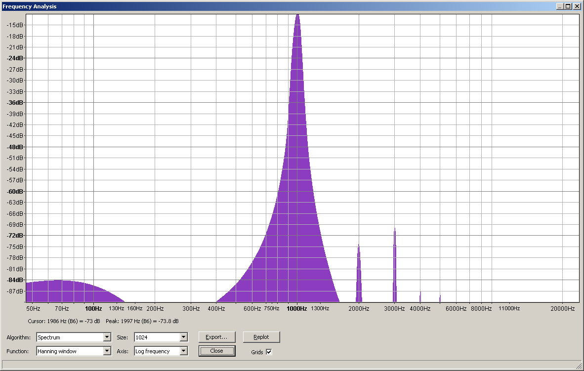
The amplifier output for 140 dB SPL had minimal distortion. The
second harmonic was 61dB down and the third 58 dB down. An
Audacity spectrum analysis is here:
sp1.png.
The output of the mic pre-amp went via a capacitor, into a pot, and
then to a Fostex VC-8 8 channel, 20 bit ADC unit. The resulting
48 kHz digital audio was saved to .WAV files for analysis.
Grounded Source mode - very limited high SPL capability
I think these FETs for electret
microphones are generally designed to be used in a Grounded Source
configuration, which is shown at the left:
With a 6.8 k load resistor, this
capsule produced a significantly higher gain than with the Source
Follower, or the new pre-amp, but it ran into problems at relatively
low SPLs.
With a 2.5 volt supply the Drain settled at 1.541 volts. Applying
115 dB SPL altered
the average voltage to 1.486 volts, which is a significant "DC
Thump". Distortion components, relative to the first harmonic
were:
Second harmonic: -27 dB
Third harmonic: -43 dB
If the total power of these harmonics added up to a level -40 dB below
the first harmonic, this would constitute 1% Total Harmonic Distortion
(THD), a level frequently used when assessing microphone quality.
The result above, counting just the second harmonic, is about 4.5 %
THD. This is probably not so audible with a single sine wave, but
the same processes would cause objectionable inter-modulation of any
complex musical or naturally occurring sound signals at different
frequencies.
I don't have detailed notes, but raising the power supply voltage
didn't help much. This capsule, with this FET, in this
configuration is not at all suited to high SPLs. However, it is a
sensitive, simple, arrangement suitable for lower sound levels,
probably to 110 or 115 dB SPL if distortion is allowable at these
higher sound levels.
In this mode, a positive increase in sound pressure creates a negative
going output voltage. The positive pressure change results in a
positive voltage change on the Gate, which decreases the incursion of
the Gate's depletion layer into the channel. With a wider
channel, there is less resistance and the FET pulls the load resistor
to a lower voltage.
Source-Follower mode, as recommended by Transound
This is the diagram from the Transound datasheet:
In this mode, as with my new circuit, a positive change in air pressure
(positive increase in Gate voltage) leads to a positive-going output
signal.
I measured the sensitivity at about 7 mV RMS at 1 PA (94 dB SPL),
slightly below what I measured with the new pre-amp. This is
about -40 to -41 dB below 1 volt per pascal. The spec sheet's
sensitivity value is -45 +/- 4dB.
A power supply of 1.5 volts is OK for lower sound levels and the capsule is specified for a maximum level of 120 dB SPL.
Below are the results for 4.9 volts, with 6.8k load. These
consist of the change in average voltage due to the high SPL signal and
the two highest level distortion harmonics, which are the second and
the third.
The voltage of the Source with no audio signal was about 1.016 V.
The changed average voltage was always to the positive, and represents
a DC thump at the onset of loud signals.
The low initial average voltage may involve clipping of the negative
going extremes of the initial parts of a suddenly large signal. At
first, the signal cannot go low enough, since it is greater than about
1 volt peak, and the load resistor can only pull down to ground, not go
below ground. After a fraction of a second, the FET rebiases its
Gate and the average voltage rises. This higher average voltage
better accommodates the large signal without so much distortion, but
this higher than normal average voltage then will decay when the high
sound level suddenly stops, leading to another DC thump.
Here is a 15 second video of the oscilloscope, showing the DC thump very clearly with burst of 140 dB SPL 1 kHz:
dB Change
in Second
Third Notes
SPL voltage at harmonic harmonic
this SPL dB below dB below
first first
120 10 mV
-43 below -60 OK.
125 50 mV
-38
-54 OK, but a bit of
DC thump.
130 144 mV!
-31
-47 This and the rest
have
bad DC thump.
135 544 mV! -28 -37
140 1,501 mV! -30
-38 See distortion
harmonics
graph in next section.
Perhaps the 135 dB SPL results are not quite right.
Anyway, the DC thump problem probably makes this approach unusable for
quality sound recording of levels much higher than the rated maximum of
120 dB SPL.
Performance of the new pre-amp
There are no "DC Thump" problems with
the new pre-amp. The FET is always running with the same current
and voltages, so there is never a significant current flowing in our
out of the Gate to charge or discharge the capacitance of the backplate.
This avoids the most serious limitation of the two conventional approaches described above.
Distortion figures are much lower than with either of the above approaches.
One problem remains, which either does not exist or is not clearly
visible with the conventional approaches: a slow reduction in gain,
over a few seconds, during periods of very high sound level. I
discuss this fully in the next section.
As far as I know, this "gain reduction" problem is not caused by the
new pre-amp. There's no way the new circuit could do anything
much different from following the Gate voltage exactly. So the
gain reduction, which does not involve distortion, is presumably a
function of the microphone capsule itself. Maybe other capsules
wouldn't have this problem, or would have it at higher or lower sound
levels.
Here are the figures for the various sound levels:
dB Second Third Notes
SPL harmonic harmonic
dB below dB below
first first
125 -56 -62
130 -51 -55
135 -45 -47
140 -41
-43 See
distortion harmonics graph
below.
The "gain reduction" problem is not evident at 130 dB SPL. After
three or four seconds of 135 dB SPL, it causes about a 6% (0.5 dB) drop
in gain.
At 140 dB SPL, the "gain reduction" problem is more pronounced, with
about a 13% drop (1.2 dB) after three or four seconds. I think
the reduction may increase somewhat beyond this if the signal continues
for tens of seconds.
The distortion figures for 135 and 140 dB SPL are therefore of
electrical signals which are a little below the proper signal which
would be produced by a capsule with no gain changes.
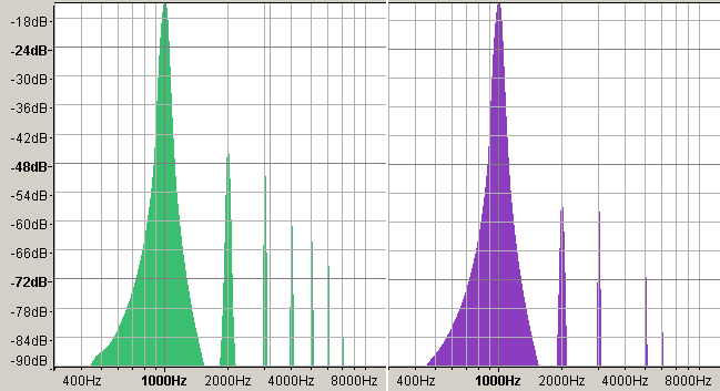
The graph below depicts the first harmonic, and then the higher
(distortion) harmonics resulting from 140 dB SPL on the left (green)
with the Source Follower mode described above, and on the right
(purple) for the new pre-amp. Both signal are actually one or two
dB below what they should be, due to the "gain reduction" problem.
The "Gain Reduction" problem at high SPLs
Observations
Later I will attempt to measure this more carefully, including at sound levels above 140 dB SPL.
This problem is clearly visible in the waveforms resulting from 140 dB
SPL 1 kHz, over several seconds, with both the Source Follower mode and
with my new pre-amp. It is easier to see with the latter due to
the absence of "DC thump" changes in the centre-voltage of the output.
I think this problem would be imperceptible at 135 dB SPL and would be
just perceptible at 140 dB SPL, except in contrived circumstances which
would make it more obvious. For instance, a continual low-level
tone, then a blast of 140 dB SPL sound for 10 seconds. When the
blast is finished, the level of the quieter tone would be quieter than
before and would rise back to normal over 5 or 10 seconds.
(Maybe this phenomena depends on temperature and humidity - these tests
were done at ordinary room temperature of about 24 C and with
not-too-high humidity.)
The image below depicts the envelope of the new pre-amp's output when a
140 dB SPL 1 kHz sine wave is switched on and off. The switch was
crude - a physical switch in series with the midrange driver.
This causes some glitches and low frequency signal at the start, unless
by chance the point of turning on the signal was at a zero crossing
point. It also causes a major glitch when I opened the switch,
since the midrange driver was electrically uncoupled and resonated
without any damping, however I have edited this glitch out.
What is important is the decline in gain over these 3.5 seconds.
It seems that the gain drifts back towards normal after a few seconds
of silence, or probably just lower levels than about 135 dB SPL.
While it is arguable a safety feature for listeners to back off the
gain with such high sound levels, this is a limitation of this capsule
and my new pre-amp.
I think it probably wouldn't matter to have occasional peaks go to 140
SPL, since these would only cause fractional dB gain decreases, which
would fade away after a few seconds. As far as I can tell, there
is no significant difference in the distortion harmonics from the start
to the end of this section of signal.
I would research this further, but it is late, good people need peace and quiet, and I am trying to wrap up this web page ASAP.
Potential explanations
As far as I know, this problem does not
involve any reduction in the gain of my pre-amp, which is fixed at 1.0
precisely, even if the FET gets somewhat different operating
conditions, which I think it does not.
Therefore I think the problem must be inherent to the capsule.
Please remember that 140 dB SPL this is 100 times the maximum power
level Transound specify. If the capsule suffered lasting damage,
we should not be surprised!
I can't imagine any mechanism which would cause the diaphragm to move
any differently. There's no evidence for an overall DC shift in the
Gate voltage - that would show up directly in the output of my
pre-amp. Such a shift could in theory reduce or increase the
gain, since adding a voltage to the backplate would add or subtract
from the electret voltage the backplate presents, capacitively, to the
rear of the diaphragm. (I plan to test the electret's effective
voltage by raising or lowering the voltage of the diaphragm until the
microphone produces no signal.)
There are only two mechanisms I can imagine at present to explain this
phenomenon. These two are tentative theories at best - I am not sure
how this could occur except by direct contact, and I think that would
result in much higher levels of distortion than are observed.
Please let me know your thoughts, directly or via the Micbuilders list.
- When the back of the diaphragm comes very close to the front
surface (the surface of the elecret with the embedded charge) the back
surface of the diaphragm may, but some mechanism, pick up some of this
charge. This would reduce the effective voltage of the condenser
microphone perfectly smoothly, without distortion. As the excess
charge drained away in a few seconds of no audio signal, or quieter
audio signal, then the normal gain would be restored.
- Likewise, and perhaps simultaneously, the front surface of the
electret layer may pick up some of what it sees as the different charge
of the back of the diaphragm.
Later I will do some experiments to try to understand this process and
to find out how much it affects several individual capsules.
~~~ooo000ooo~~~
