Special techniques for KiCad
2016-05-06 (Updated 2018-06-15) Robin Whittle
rw@firstpr.com.au 
KiCad - http://kicad-pcb.org - is a full-featured open-source schematic and PCB design program.
I am active on the KiCad Users mailing list is https://groups.yahoo.com/neo/groups/kicad-users/info .
There is also a web-based KiCad Users Forum: https://forum.kicad.info . This has a higher volume of messages than the mailing list, but I prefer mailing lists for in-depth discussions. That said, the mailing list is falling into disuse and most of the action is in the Web forum.
(2023-09-02 mini update: I am not sure how relevant all this material is to Kicad in 2023. I haven't done any work with it since 2018. Today I updated a link to Andrew Tweddle's site, which is now https://pcbsynergy.com .)
Sections 01 to 08 below were originally written in May 2016 for KiCad 4.0.2. In early October 2017 I updated this page where necessary for the current version 4.0.7. (See archive.org link for the 2016 version of this page.)
In January 2018 I added a big new section on Design for Manufacturability. This primarily concerns the footprint library. I can't continually update every part of these pages, so please note that they were written at various times and will not be totally up-to-date with the latest KiCad developments.
I use KiCad on Windows 7 since my main PC is Windows 7 and has four 1920x1200 monitors. In principle I could run it under Linux, but at present (2017-10-09) the latest version of KiCad (4.0.7) is only available for Debian if I install the current Testing version of Debian, Buster, which would do under Virtual Box . . . and for some reason I was unable to do this.
Contents of this page:
| #kpv |
01
-PCBVal: Adding a field to schematic components so their value on
the PCB can be different from their value on the schematic. |
| #bomw |
02 - Creating a simple, ungrouped, Bill of Materials (BOM) from KiCad running under Windows 7. This also links to other pages for creating a grouped BOM, and for using some Python scripts to generate BOMs. |
| #bomf |
03 - Initial ideas for fancy BOMs with part numbers and stock numbers |
| #tfn |
04 - Template Field Names in Eeschema 4.0.2-stable - later known as Default Fields |
| #kds |
05 - Data Structures for KiCad - especially for generating BOMs |
| #conv |
06 - Converting from old Protel files, including from Autotrax for DOS (1989). |
| #smtf |
07 - Deciding exactly on SMT footprints using standards documents, software etc. |
| #links |
08 - Links to other sites. |
Four other pages:
kicad-data-structures/
kicad-pcb-value/
kicad-python-bom-scripts/
kicad-design-for-manufacture/
How I iteratively design the schematics
and PCB, using schematic library symbols which already specify a
particular footprint, which is not how KiCad usage is described in the
documentation.
Also, some basic BoM (Bill of Material) techniques.
Also, some basic BoM (Bill of Material) techniques.
kicad-pcb-value/
A C++ program, with source and a
Windows executable, to process the netlist file generated by Eeschema
so that the contents of a component's PCBValue field can override the
value in the Value field. The intention of this is the schematic
contains the alternative, and typically shorter, text in cases where
this is desired, with the alternative text appearing in the Eco1.user layer which is used to create a graphic image to as a human-readable guide to manual and automated SMT assembly.
kicad-python-bom-scripts/
How I installed a Python interpreter on
Windows 7 and ran the KiBoM Python script, which does a great job of
producing a collated Bill of Materials (it is driven by Eeschema), with
multiple componentssharing the same footprint and value collected into a single spreadsheet line.
kicad-design-for-manufacture/
This page primarily concerns how I
created footprints using Library Expert, from PCBLibraries.com,
modifying the exported file in certain ways and importing it into KiCad
for my personal footprint library.
It also concerns how I use the various layers of Pcbnew, in particular Eco1.user, which I use for a printed guide to hand and automated SMT assembly, with simple rectangular outlines and a few numbers such as 2204 or 104 or text denoting the value of each SMT component. This works well with the PCBValue field in my schematic library symbols, using the kicad-pcb-value program.
This will later include details of checking the component placement file, and other things regarding automatic assembly. If all goes well I will be doing an automated assembly run later in 2018.
#kpv
01 - PCBVal: Adding a field to schematic components so their value on the PCB can be different from their value on the schematic
On 2016-04-22 I asked on the mailing
list about how I could have a particular device in the schematic have
one value displayed there, such as BZT52H-B5V6
but export via the netlist some other value, including perhaps just a
space which is invisible, to the PCB program, so that the value field
for the matching device in the PCB is different, such as 5V6 or not visible at all, including as gray "invisible" text on the Pcbnew screen.
In the absence of an answer, I developed a way of doing it:
This works fine for me.
Two usage scenarios are explained in the source code and in the page linked to below. Below that link are two more usage scenarios. The program to do this is public domain C++, with 64 bit and 32 bit Windows executables. The source code is plain C++ and so can be compiled for Linux or any other OS. Please see this directory:
A third usage scenario:
The TDK part number is CGA5C2C0G1H103J060AA and Mouser's part number is C820-CGA5C2C0G1H103J. I need one of these in the BoM, but I don't want these cluttering the schematic or the PCB, including in gray "invisible" text when designing the PCB. (See also the fancy BoM section below: #bomf .)
Initially, I use the full TDK part number for the schematic component's value, make it invisible in the schematic, add a PCBValue field, set its value to 0.01uF and make this visible in the schematic with a font size I like. The latter value now appears in both the schematic, the PCB design and PCB itself, where it is the "value" of the component in the PCB.
A fourth usage scenario:
In the absence of an answer, I developed a way of doing it:
1 - Add a new field named PCBVal to
the device in the schematic. (This and the following step can
also be done to a component/part in the Eeschema component library.)
2 - Set the value of this field to whatever I want, such as 5V6 or just a space " ", since it cannot be empty.
3 - Generate a netlist in the usual way from Eeschema. The netlist contains the new field information.
4 - Process the netlist with a special program to make a modified netlist file in which the contents of (technically the value of) the value field for each component is copied from its PCBVal field.
5 - Read the modified netlist into Pcbnew.
This works fine for me.
Two usage scenarios are explained in the source code and in the page linked to below. Below that link are two more usage scenarios. The program to do this is public domain C++, with 64 bit and 32 bit Windows executables. The source code is plain C++ and so can be compiled for Linux or any other OS. Please see this directory:
A third usage scenario:
I have a 0.01 uF SMT capacitor in a
3216 (metric) 1206 (imperial) package. It is no use having "0.01uF" in
the BoM (Bill of Materials) since there are a plethora of capacitor types. I need a COG
(AKA NPO) 5% one, not some X7R device whose capacitance varies
enormously with temperature and/or voltage.
(See Mark Fortunato's widely cited article
from EDN in 2013 [ link ] http://pdfserv.maximintegrated.com/en/an/TUT5527.pdf "Temperature and Voltage Variation of Ceramic Capacitors, or Why Your 4.7µF Capacitor Becomes a 0.33µF Capacitor".)
The TDK part number is CGA5C2C0G1H103J060AA and Mouser's part number is C820-CGA5C2C0G1H103J. I need one of these in the BoM, but I don't want these cluttering the schematic or the PCB, including in gray "invisible" text when designing the PCB. (See also the fancy BoM section below: #bomf .)
Initially, I use the full TDK part number for the schematic component's value, make it invisible in the schematic, add a PCBValue field, set its value to 0.01uF and make this visible in the schematic with a font size I like. The latter value now appears in both the schematic, the PCB design and PCB itself, where it is the "value" of the component in the PCB.
A fourth usage scenario:
I want a value like 0.068uF for the schematic, but for space reasons, on the PCB: 683.
On 2016-04-25 I mentioned this and some of the sections below on the KiCad Users Forum:
There are various other discrepancies
between what we think of at the schematic level, what we think of on
the PCB design, and what
we want when ordering parts, getting quotes on assembly etc. For
instance, from a schematic point of view, I want a 28 pin DIP
microcontroller, with its pin functions being based on the innate pin
functions of the chip, but specialised for the particular functions
they perform when my firmware is running. The same goes for the
PCB design in most respects, since I want to see those pin functions
when laying out tracks.
Yet at a parts ordering and PCB automated/manual (or at least outsourced to another company) assembly stage, there will be a 28 pin DIP socket on the board, and the microcontroller will be plugged in later.
Another discrepancy arises when we consider the PCB might have two or more versions for different applications. Perhaps they will all be assembled the same way, or perhaps differently. Perhaps there will be final components added by hand which differ between the versions. Perhaps the versions will require different components in particular positions, or at least different firmware files to be used for programming microcontrollers and PLDs etc. The mounting or not of particular components in multiple variations of the physical PCB are handled well by the Python-based KiBOM system for generating B0M files, which I mention at: kicad-python-bom-scripts/
By careful and consistent use of schematic component fields, and potentially by manipulating the resulting netlist with a program such as kicad-pcb-value, we may be able to achieve some systematic ways of dealing with these challenges, rather than relying on manual processes. In the next section (#alternetlistbeforebomgeneration), I contemplate how some program of ours could be called as part of the BoM generation system, to alter the data found in the just-produced .xml file, to create a different .xml file which would be fed to xsltproc.exe, or to some other BoM generation system such as a Python script.
#bomwYet at a parts ordering and PCB automated/manual (or at least outsourced to another company) assembly stage, there will be a 28 pin DIP socket on the board, and the microcontroller will be plugged in later.
Another discrepancy arises when we consider the PCB might have two or more versions for different applications. Perhaps they will all be assembled the same way, or perhaps differently. Perhaps there will be final components added by hand which differ between the versions. Perhaps the versions will require different components in particular positions, or at least different firmware files to be used for programming microcontrollers and PLDs etc. The mounting or not of particular components in multiple variations of the physical PCB are handled well by the Python-based KiBOM system for generating B0M files, which I mention at: kicad-python-bom-scripts/
By careful and consistent use of schematic component fields, and potentially by manipulating the resulting netlist with a program such as kicad-pcb-value, we may be able to achieve some systematic ways of dealing with these challenges, rather than relying on manual processes. In the next section (#alternetlistbeforebomgeneration), I contemplate how some program of ours could be called as part of the BoM generation system, to alter the data found in the just-produced .xml file, to create a different .xml file which would be fed to xsltproc.exe, or to some other BoM generation system such as a Python script.
02 - Creating a simple, ungrouped, Bill of Materials (BoM) from
KiCad running under Windows 7 (with links to other pages regarding more advanced types of BoM)
Here is a little cheatsheet on how to
generate a simple BoM when running Eeschema 4.0.7 under Windows 7.
The Eeschema user manual (2017-08-24 on 2nd page of PDF) instructs (14.3.5) how to do it under
Linux, but it is not immediately apparent how to do it under
Windows. The following description uses the default installation location for KiCad 4.0.7, which for me was: C:\Program Files (x86)\KiCad\ .
This is for the simplest BoM, with a line for every individual component, using the simplest BoM generation translation file bom2csv.xsl. See below #kds for generating a BoM with each line containing potentially multiple components with the same value and footprint. See a separate page kicad-python-bom-scripts/ for my exploration of some Python scripts to generate further more advanced types of BoM.
There is one line for each one or more component where all components with matching Value and Footprint fields are listed on the one line. I am not sure about the order of the lines. It is easy to sort them in Excel (link). In Libre Office Calc, select the whole spreadsheet and: Data > Sort > Options > Range contains data labels; OK. In Notepad++, select all but the top line and: Edit > Line Operations > Sort Lines Lexographically Ascending.
For my project, the columns were:
This means that some fancy techniques can easily be implemented with additional fields in some or all components, as mentioned in the next section.
#bomwlinks
This BOM CSV file does not collate similar components into a single line See the third dot-point below for a way of achieving this. There are various promising approaches to be found with a Google search for:
Here are some other KiCad BOM generation links:
This is for the simplest BoM, with a line for every individual component, using the simplest BoM generation translation file bom2csv.xsl. See below #kds for generating a BoM with each line containing potentially multiple components with the same value and footprint. See a separate page kicad-python-bom-scripts/ for my exploration of some Python scripts to generate further more advanced types of BoM.
- Click the BoM icon on the top toolbar.
- Click
the Add Plugin button. This opens a file selection window for the
directory (if not, then navigate to here, or wherever your KiCad system
is installed):
C:\Program Files (x86)\KiCad\bin
- Select the program there xsltproc.exe .and click "Open".
- Give this "plugin" (really a bunch of configuration data, specifying a
plugin name and matching command line) a name, such as "XLSTPROC BOM".
The default command line:
"C:\Program Files (x86)\KiCad\bin\xsltproc.exe" < "%I" > "%O"
is not at all what we want.
- We need xsltproc.exe to use one of the two supplied translation files which works from the intermediate netlist file
to create a CSV format BoM file:
C:\Program Files (x86)\KiCad\bin\scripting\plugins\bom2csv.xsl
C:\Program Files (x86)\KiCad\bin\scripting\plugins\bom2grouped_csv.xsl
The first one is the one mentioned in the manual, and which I used in this cheatsheet in 2016. Here we use it again, since it produces a simple result, one line per component, which enables us to check various things, even if it is not the ideal BoM for purchasing, cost estimation etc. The second produces a BoM which is sorted in a way which I find more useful, but please see below #kds for how to use this, the bugs I found in its operation, and a fixed up version which for works fine for me.
Edit the command line to be as follows, all on one line, with a space for the line break you see in this web page:
"C:\Program Files (x86)\KiCad\bin\xsltproc.exe" -o "%O.csv" "C:\Program Files (x86)\KiCad\bin\scripting\plugins\bom2csv.xsl" "%I"
This text, in a single line, is in this file: kicad-sorted-bom-command.txt .
- Close this dialogue box with the "Close" button.
- With
the relevant schematic project open in Eeschema (for
instance Eeschema is editing the root - top level - schematic in an
hierarchical set of schematics, but it doesn't matter which
schematic is being edited), I can now
generate a BoM by clicking the BOM icon in the top toolbar (or Tools > Generate Bill of Materials), selecting
this plugin by name from the list ("XLSTPROC BOM") and clicking the
"Generate" button. In the bottom section of the "Bill of
Material" dialogue box, the full command text appears, followed by
"Success".
(There will be a permission error if a BoM file by the same name as to be
generated is currently opened for writing, such as by a spreadsheet program, since this file
needs to be deleted before a new one of the same name can be written in
its place.)
- An intermediate netlist file, in XML format, is generated in the above directory: D:\PCB\ABC\XYZ.xml .
#alternetlistbeforebomgeneration
At this point, we could in principle create a processed version of this file by altering the above command string to run some program of our own creation, using XYZ.xml as an input (by way of "%I" which Eeschema will expand to be the name of the just-created .xml file creating some other file, whose name we use at the end of the plugin's command string, in place of "%I".
- xsltproc runs with its first two arguments specifying an output file D:\PCB\ABC\XYZ.csv , the third argument being the above-mentioned bom2csv.xsl
file, which contains the conversion instructions, and the fourth
argument being the name of the the just-generated intermediate netlist file. The
command line, with this example, which appears in the window after I
click the "Generate" button, is (2017-10-04, 4.0.7):
"C:/Program Files (x86)/KiCad/bin/xsltproc.exe" -o "D:/PCB/DF-5-0/DF-5-0.csv" "C:/Program Files (x86)/KiCad/bin/scripting/plugins/bom2csv.xsl" "D:/PCB/DF-5-0/DF-5-0.xml"
This shows that Eeschema has interpreted the "%I" in the "plugin" text above by expanding it to be a file name using the name of the current project, plus .xml, this being the argument which specifies xsltproc's input file.
- The output CSV file is written into the project directory by xsltproc.exe.
There is one line for each one or more component where all components with matching Value and Footprint fields are listed on the one line. I am not sure about the order of the lines. It is easy to sort them in Excel (link). In Libre Office Calc, select the whole spreadsheet and: Data > Sort > Options > Range contains data labels; OK. In Notepad++, select all but the top line and: Edit > Line Operations > Sort Lines Lexographically Ascending.
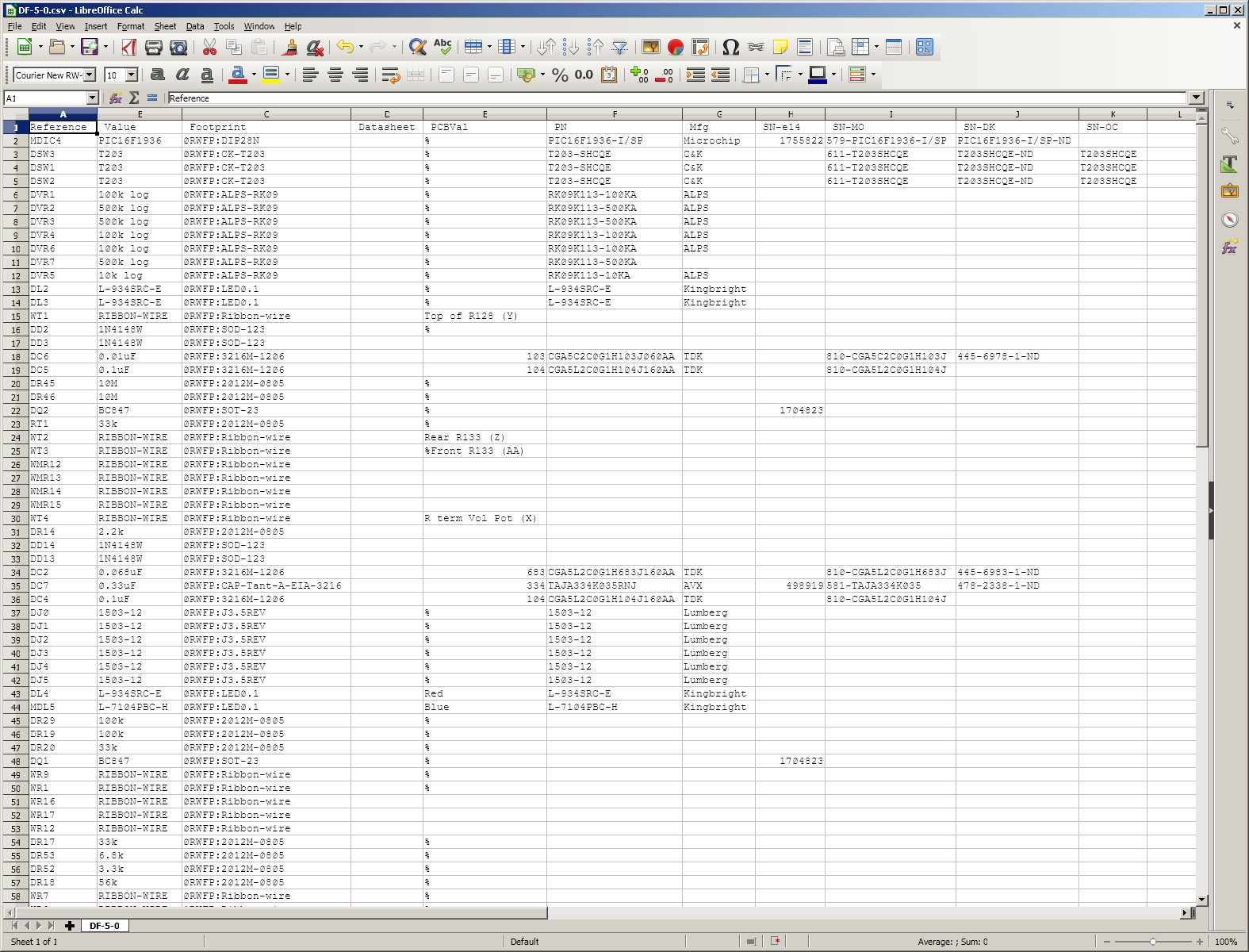
For my project, the columns were:
- Reference (e.g. "U3").
- Value. This is whatever is in the Value field, which every component has.
- Footprint. This is a library nickname, a colon, and the footprint name within that library.
- Datasheet. (I don't have anything in this field for my components.)
- PCBVal. Because some of my components have a field called PCBVal, which I added as mentioned above: #kpv, there is a column labeled PCBVal in the spreadsheet, with the value of this field for every component which has this field.
- Likewise some other columns for other fields some or all
the components had, which are stock numbers for various component
retailers.
This means that some fancy techniques can easily be implemented with additional fields in some or all components, as mentioned in the next section.
#bomwlinks
This BOM CSV file does not collate similar components into a single line See the third dot-point below for a way of achieving this. There are various promising approaches to be found with a Google search for:
BoM collate KiCad
or BoM grouped KiCad
Here are some other KiCad BOM generation links:
- Python scripts: https://github.com/hwstar/BOMtools
. A Python interpreter is normally part of a Linux installation,
but needs to be installed specifically for Windows 7. See the
page kicad-python-bom-scripts/ for more on this.
- https://github.com/SchrodingersGat/KiBoM The Python-based KiBoM system, which I explore in the kicad-python-bom-scripts/ page.
- https://rheingoldheavy.com/category/education/kicad/ Two articles by Daniel Nietzsche
on sophisticated BoM generation with KiCad, but it is probably best to
start with his Design for Manufacture in Kicad articles. It is
clearly a major project to design and implement the requisite
bureaucracy, much of it in KiCad schematic components and their library
representations, which enables the generation of various types of BOM,
such as for ordering some or all parts, getting quotes, creating files
for pick-and-place machines etc.
- https://github.com/akouz/KiCadBOM Pascal program reads from schematic files.
- https://forum.kicad.info/t/bom-grouped-by-reference/261/15
Wolf Walters modified the standard bom2csv.xsl translation program for grouping (collating) components of the same
type. I found this new translation program bom2groupedCsv.xsl to be Most Satisfactory as Dr Beaker (7:40 at https://www.youtube.com/watch?v=Snh1b7h2sMA) would say. More details on this in #kds.
- Andew Tweddle https://pcbsynergy.com (previously members.iinet.net.au/~sarason/) has a free (executable, not source code) PCBSynergy Windows
program which accepts input from KiCad,
Altium/Protel, Eagle, PADS and Orcad and generates a variety of BoM
files to help with costing and purchasing of parts. It also
generates files for a variety of SMT assembly machines. I have not
yet looked at this in detail. For an SMT newbie like me it would
be interesting to learn about the process of making files for SMT
machines, even if I won't be doing this directly myself.
#bomf
03 - Initial ideas for fancy BoMs with part numbers and stock numbers
I had some initial ideas here but they are superseded by those in a section below #kds Data Structures for KiCad - especially for generating BoMs links to a page which has a more detailed account of a better approach. Please see the links #bomwlinks
above for some pages which concern attempts at data organization and
BoM generation, written by people with much more experience than me.
#tfn
04 - Template Field Names in Eeschema 4.0.7
This feature is not explained properly
in the Eeschema User Manual (2016-04-26 or 2017-08-24, section
4.2.2). Preferences
> Schematic Editor Options > Template Field Names. Difficulties
with the user interface of this "Template Field Names" tab are mentioned in my bug 1389272 (2016).
The only explanation of the functionality of is:
I found little discussion of this facility on the Web. Here is my exploration trying to understand what this does.
To add an entry for Field Name, Default value and Visible/Hidden to this system:
The configuration data for these additional field names, their default values and whether they are visible or not are stored as part of the Eeschema config data. They are not part of the schematic or project files.
If I add such a default field named ABC, with visible default value def and if this is the only such default field then when I next edit a component in the schematic, I can see these, listed above the extra fields I added as described above: #bomf :
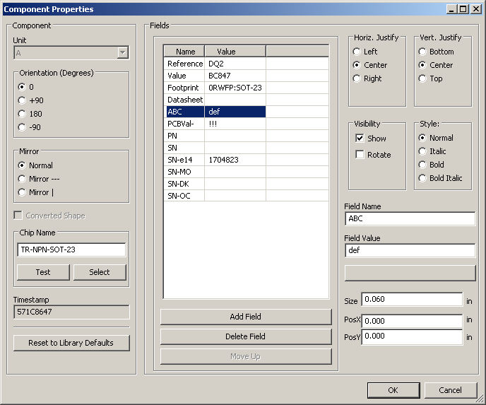
However, there is no such text ABC or def in the schematic file, if I do not actually change anything about this component, click the "Cancel" button and save the schematic project.
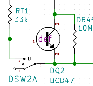
If I click the "OK" button then the component is changed, the def text appears in the centre of the component:
The saved schematic file is changed by the addition of a line, in this case field 4, with the previously existing fields 4 to 10 having their number incremented:
So my understanding is that these Template Field Names will be added to every component in the schematic which is edited, even just by opening the edit dialogue box and clicking OK. Once this has happened, the edit dialogue box looks identical to how it did previously.
This functionality is repeated in the Eeschema component library editor ("Schematic Library Editor" from the KiCad program, it calls itself in the Windows frame: "Part Library Editor"), using the T button (Add and remove fields and edit field properties" on its top toolbar, once the changed library file has been saved, and with live update to the in-memory version of the library Eeschema uses even if the library file has not been changed yet, but if the "upwards green arrow" button ("Update current component in current library") in the top toolbar of the Schematic Library Editor is clicked.
So this facility is a quick way of adding new fields to components in schematics and schematic libraries, by editing each such component and clicking "OK", with or without any changes to the visibility of value of the fields which are added by this process.
On 2016-04-26 I suggested (bug report https://bugs.launchpad.net/kicad/+bug/1575100) a revision to the Eeschema user manual for the explanation of "Template Field Names", then known as "Default Fields" in the latest nightly. No-one seemed to be interested in this. Here is an updated version, using the original and now current terminology "Template Field Names":
The only explanation of the functionality of is:
You can define custom fields that will exist by default in each component (even if left empty).
I found little discussion of this facility on the Web. Here is my exploration trying to understand what this does.
To add an entry for Field Name, Default value and Visible/Hidden to this system:
- Click the "Add" button. This adds a new entry, which
appears to us as a new line in the main section of this tab. The
line will show "Fieldname", "Value" and "Hidden", which is the state of
these three items in the just-added line
- Click on the line just added, or whichever line is to be
edited. The state of this line's three items are copied to the
"Field settings" section below the main section. There they can
be edited by selecting, deleting and typing new text (the first two) or
for the third one, "Visible" ticking or unticking a tick box.
- When all changes are made, click "OK".
The configuration data for these additional field names, their default values and whether they are visible or not are stored as part of the Eeschema config data. They are not part of the schematic or project files.
If I add such a default field named ABC, with visible default value def and if this is the only such default field then when I next edit a component in the schematic, I can see these, listed above the extra fields I added as described above: #bomf :
However, there is no such text ABC or def in the schematic file, if I do not actually change anything about this component, click the "Cancel" button and save the schematic project.
If I click the "OK" button then the component is changed, the def text appears in the centre of the component:
The saved schematic file is changed by the addition of a line, in this case field 4, with the previously existing fields 4 to 10 having their number incremented:
$Comp
L TR-NPN-SOT-23 DQ2
U 1 1 571C8647
P 10000 1950
F 0 "DQ2" H 10050 1600 50 0000 L BNN
F 1 "BC847" H 10050 1500 50 0000 L BNN
F 2 "0RWFP:SOT-23" H 10010 1810 10 0001 C CNN
F 3 "" H 10000 1950 50 0000 L CNN
F 4 "def" H 10000 1950 60 0000 C CNN "ABC"
F 5 "!!!" V 10000 1950 50 0001 C CNN "PCBVal-"
F 6 " " H 10000 1950 50 0001 L BNN "PN"
F 7 " " H 10000 1950 50 0001 L BNN "SN"
F 8 "1704823" H 10000 1950 50 0001 L BNN "SN-e14"
F 9 " " H 10000 1950 50 0001 L BNN "SN-MO"
F 10 " " H 10000 1950 50 0001 L BNN "SN-DK"
F 11 " " H 10000 1950 50 0001 L BNN "SN-OC"
1 10000 1950
1 0 0 -1
So my understanding is that these Template Field Names will be added to every component in the schematic which is edited, even just by opening the edit dialogue box and clicking OK. Once this has happened, the edit dialogue box looks identical to how it did previously.
This functionality is repeated in the Eeschema component library editor ("Schematic Library Editor" from the KiCad program, it calls itself in the Windows frame: "Part Library Editor"), using the T button (Add and remove fields and edit field properties" on its top toolbar, once the changed library file has been saved, and with live update to the in-memory version of the library Eeschema uses even if the library file has not been changed yet, but if the "upwards green arrow" button ("Update current component in current library") in the top toolbar of the Schematic Library Editor is clicked.
A brief rant of frustration with KiCad's user interface:
The way the KiCad programs operate, with one or more toolbars with symbols to identify the buttons, drives me nuts.
It would be OK if the symbols had identifying text as well, or if there were no symbols and just identifying text. The mouseover text is not a proper substitute for text labels for buttons.
I want to be able to see what each button does without having to remember anything about what these symbols mean. My brain is full of stuff as it is, and I don't want to have to learn and remember such things, especially as some buttons are never, or rarely used, and since months may pass between periods of using these programs. Furthermore, if I write, in my personal cheatsheets or here, a description of which button to press, that will be a textual description and it should take no more than a second or two to look at the toolbar to find which button is being referred to. This is not possible in the KiCad program. The reader is forced to remember which symbol that button has, or use mouseovers successively, which is very slow and transitory, to identify the button.
It doesn't
help that the one concept has multiple names within the program.
This is a common problem in any complex system. The one program
might be called "Part library editor" or "Schematic Library
Editor". What is the term for a schematic thing in a
library? What is the term for such a thing placed on a schematic
sheet? "Part"? "Component"?
So this facility is a quick way of adding new fields to components in schematics and schematic libraries, by editing each such component and clicking "OK", with or without any changes to the visibility of value of the fields which are added by this process.
On 2016-04-26 I suggested (bug report https://bugs.launchpad.net/kicad/+bug/1575100) a revision to the Eeschema user manual for the explanation of "Template Field Names", then known as "Default Fields" in the latest nightly. No-one seemed to be interested in this. Here is an updated version, using the original and now current terminology "Template Field Names":
#bug1575100text
"Template Field Names" are a mechanism for easily introducing additional fields into components in schematics or component definitions in schematic libraries. This can be accessed from Eeschema by clicking the Preferences menu, then the "Schematic Editor Options" item, and from there selecting the "Template Field Names" tab,
Each set of three items consists of a field name, a default value for this field - which can be empty - and a flag which controls whether the value of this field will initially be visible in the schematic editing screen and the printed schematic.
These configuration items are part of the Eeschema configuration and are not part of any schematic sheet or project.
The one or more sets of items specified here do not exist in any components in schematics or in schematic libraries until each such component is edited and the "OK" button is pressed in the edit dialogue box. Then, the one or more sets of Template Fields are added to the already existing fields for this component, starting at field 4, with any previously existing fields 4 and above being renumbered accordingly. Changes can be made to the value and/or visibility flag during this initial edit session or at any subsequent time.
Later changes to the default value of a Template Field will not affect the value of fields which have already been added to components. Once one or more fields have been added to a component, each also has parameters for position, size and orientation of the text, when displayed in the schematic.
To create and edit these sets of items, each set being a "Template Field", use the "Add" button to add one or more sets of items to the upper section of this the Template Field Names tab. Once one or more sets are there, select one of them, and edit its Name, Default Value and Visible/Invisible status in the lower section of this tab. The "OK" button saves any changes to this set, as does selecting another set.
#kds
05 - Data Structures for KiCad - especially for generating BoMs
Please see the separate page kicad-data-structures/
for an account at my initial attempts at creating and populating fields
in Eeschema schematic and library components for the purposes of
helping with parts ordering etc.
I was able to get a grouped BoM (all components which are the same accounted for on a single line) as a CSV file, very nicely, with Wolf Walter's .SLT file. This worked fine with the new fields I added to schematic components.
I was able to get a grouped BoM (all components which are the same accounted for on a single line) as a CSV file, very nicely, with Wolf Walter's .SLT file. This worked fine with the new fields I added to schematic components.
#conv
06 - Converting from old Protel files, including from Autotrax for DOS (1989)
On 2016-02-13 I started a thread on converting from old DOS Autotrax PCB files, (link to the narkive.com copy of this thread, which is actually on a Yahoo Grouls mailing list)
via Protel 99, through various other stages to generate KiCad PCB
files. This is also a way of transferring PCB components
("footprints" in KiCad parlance) from these old systems into PCB files
from which they can be added to the KiCad footprint library. The
techniques discussed in this thread lead to a bug report https://bugs.launchpad.net/kicad/+bug/1547822 which resulted in Eldar Khayrullin improving the import facility for P-CAD ASCII files, which can be exported from Altium.
So the path of conversion is from DOS Autotrax to Protel 99, and from there to a free trial version of Altium, which exports P-CAD ASCII files which can be imported reliably into KiCad. Initially I used Eagle in one of the later steps too, but the improved import facility makes this unnecessary.
On 2018-06-15 I used the 2017-11-18 revision ff5ee05de Windows nightly to import a P-CAD ASCII file I had previously generated from a trial version of Altium16.0.6 (as described in the mailing list thread, from a Protel 99 export of an imported DOS Autotrax PCB file) and the results were good. This KiCad was compiled after the above bug was fixed. I used File > Import Non-Kicad Board File and from there selected the "P-Cad 200x ASCII PCB files (*.PCB)" option. I was happy with the results:
I did the same with the latest 2018-06-14 Windows nightly kicad-r10526.b82bf7c44-x86_64.exe (5.0.0-rc2-154-gb82bf7c44) and the results seemed to be the same.
Search engine bait: Protel to KiCad; Autotrax to KiCad.
#smtf
07 - Deciding exactly on SMT footprints using standards documents, software etc.
It turns out that deciding on exact
dimensions of SMT pads for resistors, capacitors, diodes, transistors -
and probably everything else - is a Black Art. This is not
the sort of problem I wanted to deal with while taking my first steps
in designing SMT boards, but it can't be avoided. I started a
thread in the KiCad Users Mailing List on 2016-02-24 about what I found
in terms of standards documents such as IPC-7351C, software and the
like which helped with these decisions. The discussion was very
fruitful.
A note to anyone starting with KiCad: be sure to establish your own libraries for both schematic components and PCB footprints (previously known and "modules"). This is not clearly explained in the documentation. This has been explained numerous times in the mailing list, most recently in discussions starting on 2016-04-19. It takes a while to understand what these libraries are and how to edit them. The GitHub libraries are a starting point - it may be a good idea to start with some of these items and modify them to suit your exact purposes. Otherwise, with a bit more experience, it can be best to start from scratch - or for schematic components with lots of pins, see the links section below.
A more recent discussion of SMT design for manufacture, particularly concerning how to make footprints with the "correct" (if there is one) orientation (angle and centroid) to suit the orientation of the component in the tape being fed to the pick-and-place machine: https://forum.kicad.info/t/hackaday-designing-for-fab-a-heads-up-before-designing-pcbs-for-professional-assembly/7886/13
#links
08 - Links
A web-based system for creating
schematic components (such as to import into the Eeschema library
editor) for large DIP devices. This is particularly handy for
creating schematic components with large numbers of pins, such as with
28 pin DIP PIC chips etc. With a text file of pin numbers and
names, a little work with the web page, I was able to make a perfectly
satisfactory schematic component:
A link farm of numerous KiCad-related sites. I will not try to duplicate it here - please check it out:
A system for using a schematic's BOM output to find prices of parts at multiple distributors:
Update history:
- 2016-04-23 - 24: Initial version: kicad-pcb-value,
conversion from Protel, resources for SMT pad design decisions and a
link.
- 2016-04-25: Added section for BOM generation under Windows and
fancy (for me as a beginner) BOM techniques involving separate fields
such as for the stock numbers at different suppliers.
- 2016-04-26: Added a section on Default Fields and more on BOMs.
- 2016-04-27: Added a section with a separate page on data structures for generating BOMs and the like.
- 2016-04-28: Minor updates and deleted the section on initial ideas on new fields.
- 2016-05-06: Added link to PCBSynergy program.
- 2017-10-08: Various changes for KiCad 4.0.7.
- 2018-01-02: Added the design for manufacture page and created descriptions of this and the other pages.
- 2018-06-15: Added note about mailing list falling into disuse. Updated section on converting from old Autotrax PCB format.
© Robin
Whittle 2016-2017 –
First Principles and Real World Interfaces