Some Transsound electret microphone capsules from JLI Electronics - photos, and dismantling three of them
|
Robin Whittle rw@firstpr.com.au 2011-07-04
<<< To the parent page which links to
another page concerning a high-performance pre-amp for the TSB-140AO,
and others with an inbuilt FET with separate connections for Source and
Drain.
2020-07-26 update. Microphone Builders
(MicBuilders) is a discussion mailing list established in 2004,
initially at Yahoo Groups. It is now at groups.io, which is an
excellent system for discussion groups with full email list
capabilities, searchable web archives and web-only posting
facilities. I find it better than Google Groups - and Yahoo
Groups has been retired. http://groups.io is written and run by Mark Fletcher, who wrote and ran ONElist, which merged with eGroups and then became Yahoo Groups.
I have had the very best experiences with this mailing list:
Contents
#explanation Rough explanation of back electret microphones.
#photos Photos and links to datasheets.
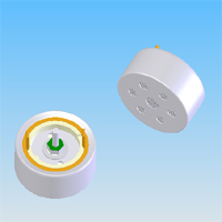
#TSB-120A Now the
TSB-120A1-GP:12mm
uni-directional with internal FET and load resistor. Black case
intended to be the outer part of the complete microphone assembly.
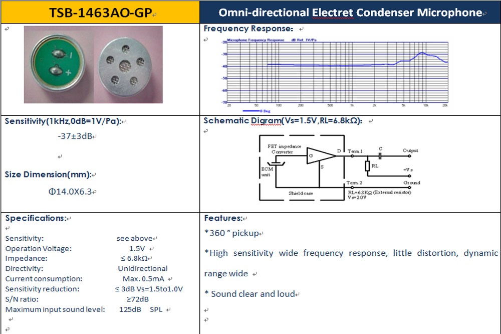
#TSB-140A Now the
TSB-140A25-GP: 14mm uni-directional capsule with internal FET with independent source and drain connections.
#TSB-140AO Now the
TSB-1463AO-GP 14mm
omni-directional capsule with internal FET with independent source and
drain connections. In July 2011, this appears to be the largest
omni-directional capsule Transsound makes.
#TSB-1460A 14mm uni-directional capsule without FET. In July 2011, this appears not to be available from Transsound.
#TSB-160A Now the
TSB-160A-GP: 16mm unidirectional capsule without FET.
#TSB-165A 16.5mm unidirectional capsule without FET. In July 2011, this appears not to be available from Transsound.
#TSB-2555A Now the
TSB-2555A-GP: 26mm unidirectional capsule, without FET.
Update history
2009-09-18 Page established.
2009-09-25: TSB-160A connections.
2009-09-28: TSB-140AO and TSB-2225A capacitance.
2009-10-21: TSB-120A FET 2SK596.
2011-07-04: New datasheet URLs and local copies of these, also a new section on
measuring the polarization voltage of the electret element.
Background
These pages contain photos and other information for people with a
technical interest in how microphones work. Some images were corrected for pincushion / barrel distortion with
PT-Lens . The background is 1mm graph paper and the camera is a Sony DSC-F707.
In mid-2009 I purchased some Transsound electret capsules from
JLI Electronics in the USA:
(In July 2011 the page above does not list all their products, so it is best to email them or call them by phone.)
The index page at the Transsound site for these and other larger electret microphones is:
The company is called Transound Electronics Co. Ltd. (one 's') but the .com domain has two 's's.
These capsules are being discussed on the Micbuilders mailing list:
Several list members really helped me understand these microphones.
Please see the Micbuiders list from 2009-09-18 for discussion of some
preliminary tests I did on some of these capsules.
A Chinese company which can supply Transsound capsules is
Zhejiang Ningbo Longxing Electronic Co. Ltd.
They have a
Uni-ECM-LX26070W which appears to be the same as the TSB-2555A-GP.
They also have some single and dual diaphragm capsules (electret, I
assume, rather than requiring an external polarizing voltage) which are
34mm in diameter, and appear to have a diaphragm about 24mm in
diameter. I can't find any such microphone at the Transsound
site. These are the
LX34-1 (single diaphragm, unidirectional) and the
LX34-2 dual diaphragm, which depending on how the two signals are used, can be omni-directional, uni-directional or bi-directional.
Rough explanation of back electret microphones
Neumann's
Microphones for Studio and Home-Recording Applications (4th edition, 1999
http://www.neumann.com/download.php?download=docu0002.PDF) is a good reference for understanding microphones.
All these microphones are "back electrets". There is
supposedly a
"front electret" design, which I don't understand. The main
alternative to the "back electret" approach is the "foil-type" or
"diaphragm-type", which I attempt to describe in the next
paragraph. These pages at Google Books contain a diagram and
explanation too:
Standard Handbook of Audio and Radio Engineering.
Many electret microphones were made, and I guess some may still be
made, with the diaphragm being an electret film. The front was
metalized and the back was not. The metalized layer is connected
to ground. The electret polarization gives the back of the
diaphragm a charge, much like that back being a conductive sheet with a
voltage on it. (I will assume a positive charge.) Very
close behind the back surface of the diaphragm is a metal
backplate. (Or a conductive plastic back-plate - I have an old
Panasonic 9.7 mm omni microphone like this.) When the sound moves
the diaphragm closer to the backplate, a temporary positive voltage is
induced. (Electrons are attracted to the front surface of the
backplate, due to the closer presence of the positive charge on the
back of the electret diaphragm.) When the diaphragm moves
forwards, there is less capacitance from its rear surface to the
backplate, and a negative voltage is induced. These voltage
changes are like sending a signal through a capacitor of a few
picofarads or a few tens of picofarads. So there needs to be a
very high impedance amplifier right there to buffer the signal so it
can sent somewhere else.
The microphones shown here use the "back electret" principle. The
diaphragm is not an electret. It is (I assume) Mylar with an
aluminium layer on the front. This layer is grounded and the back
of the Mylar has no charge built into it. So the back surface of the diaphragm is capacitively
coupled to ground, with the mylar being the insulator of the
capacitance.
The backplate has on its front surface a thin layer of electret
material, with the top surface having a negative charge. This is
somewhat like putting down an insulating layer and then a conductive
layer, and connecting a steady negative voltage to that layer, with
respect to the metal backplate.
I understand this electret layer is some kind of fluoro carbon polymer
- Teflon and the like. I understand that after it is deposited,
some kind of process (such as corona discharge) is used to permanently
alter the polymer so its front surface has a charge with respect to the
backplate. Teflon, or whatever is used, is a very stable
insulator and I understand the charge can persist for hundreds of
years. I haven't yet found good information about charge
stability of electrets. Please point me to any such information.
Please see my recent message
http://tech.groups.yahoo.com/group/micbuilders/message/11824
for how I measured the thickness of the diaphragms and spacer
rings. (I used a micrometer with mirror-polished tungsten carbide
tips - very carefully.)
Model            Diameter   Diaphragm  Spacer   Sensitivity
                            thickness  ring

TSB-120A   Uni    8.0 mm    ~3 um      ~75 um   -46 dB +/- 4

TSB-140AO  Omni  10.5 mm    ~6 um      ~60 um   -45 dB +/- 4

TSB-2555A  Uni   21.0 mm    ~6 um      ~75 um   -40 db +/- 4
Googling reveals that 3 um and 6 um are popular thicknesses of diaphragms of (non-electret) condenser microphones.
I have some older, definitely not back electret, Panasonic 9.7 mm omni
electret cartridges. Their backplates have no insulating
coating. Their diaphragms are ~10 and ~15 um thick.
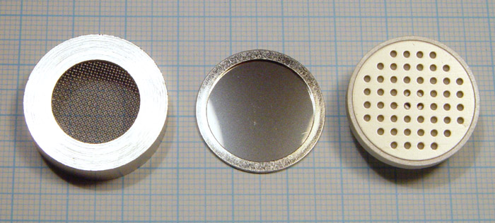
Photos
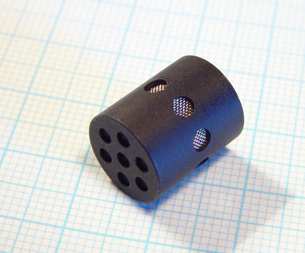
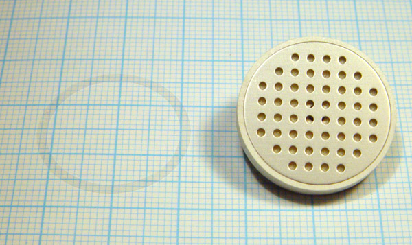
TSB-120A
TSB-140A
TSB-140A: (This datasheet was valid in 2009 but does not exist July 2011:
http://www.transsound.com/work_show.asp?work_id=395 I don't have a copy.)
Unidirectional (cardioid) 14mm with internal FET giving access to both source and drain.
In July 2011, this particular microphone is replaced by a functionally equivalent one with different rear connections:
TSB-140A25-GP http://www.transsound.com/work_show.asp?work_id=488. I have a copy of this datasheet archived here:
2011052109473129207TSB-140A25-GP.jpg .
See below
#measuring_electret_voltage
for some notes on how these capsules, and the omni-directional
TSB-1463AO-GP capsules mentioned below, have independent connections
for the internal FET's source and drain. These three-terminal
internal FET electret mic capsules therefore resemble a two terminal
capsule after the "Linkwitz modification".
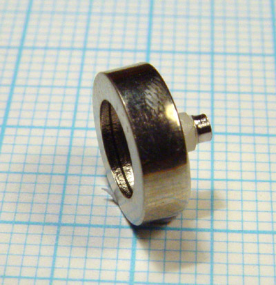
TSB-140AO
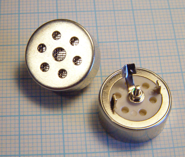
TSB-1460A
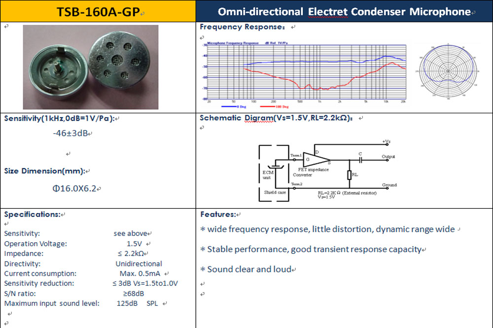
TSB-160A
TSB-160A: (Datasheet was:
http://www.transsound.com/work_show.asp?work_id=392 .)
In July 2011, this appears to be available, as the
TSB-160A-GP:
http://www.transsound.com/work_show.asp?work_id=490 The datasheet is archived here:
2011052110004597604TSB-160A-GP.jpg .
Unidirectional (cardioid) 16.1mm, without internal FET.
These did not have a solder tag on the screw - so they would be hard to
use. There is no sign of a
solder tag in the data sheet, but there is no sign of one in the
TSB-2555A datasheet, and these capsules do have one. One can't
very
well solder to the screw. It would probably not wet to solder and
I expect the heat transfer would melt parts of the capsule.
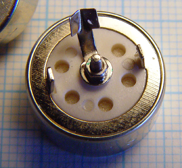
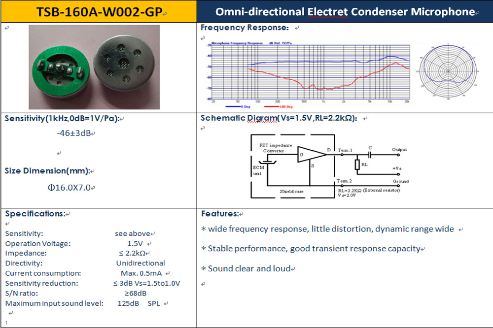
JLI Electronics wrote to me on 2009-05-25, including a PDF of the
revised spec sheet for the TSB0160A. Below is an edited version
of a drawing from that PDF, showing the addition of two solder lugs to
the new design. It is my impression from these drawings that they
have added a thin printed circuit board to the capsule. It is not
entirely clear from the drawing how Terminal 1 (the backplate) is to be
distinguished from Terminal 2 (ground). "Term.2" looks like it
has a different shape from "Term.1". It would probably be
possible to see the PCB trace, and of course a multimeter would show
which is which.
I assume they will do this for the TSB-160AO too.
There are 6 vent holes, two of which have been sealed. I guess
this is to tune the capsule in terms of resonances and/or its
unidirectional response.
Through the holes a random-weave dampening material can be seen.
In July 2011, I think the above drawing is for a unidirectional 16mm capsule with internal FET. This is now known as the
TSB-160A-W002-GP:
http://www.transsound.com/work_show.asp?work_id=491 . This datasheet is archived here:
2011052110012842910TSB-160A-W002-GP.jpg .
In mid-2009, there was an omni-directional 16mm capsule - the largest omni microphone
Transsound made - which I did not get. This has no solder
tag either.
TSB-160AO: (Old URL:
http://www.transsound.com/work_show.asp?work_id=385 .) From archive.org, its picture was:
In July 2011, as far as I can see, Transsound does not list an omni-directional 16mm capsule, with or without FETs.
TSB-165A
TSB-165A: (Old URL:
http://www.transsound.com/work_show.asp?work_id=391 .)
Unidirectional (cardioid) 16.5mm, without internal FET.
This appears to contain the same kind of open-cell foam sheet which I found inside the TSB-2555A.
In July 2011, as far as I can see, Transsound does not make any 16.5mm capsules.
However, they are available as "Uni-ECM-LX16573W" here:
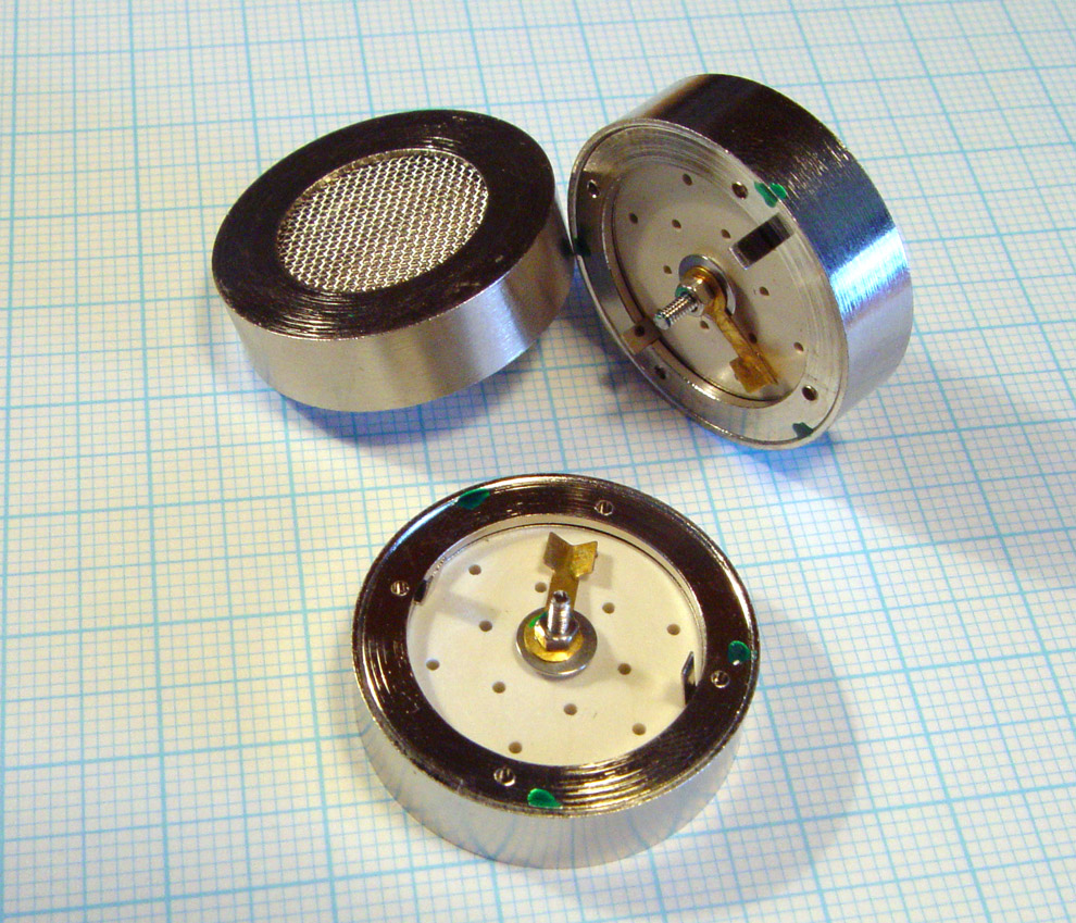
TSB-2555A
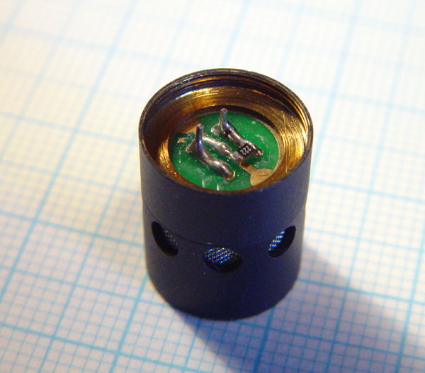
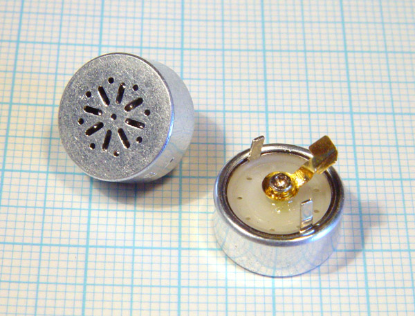
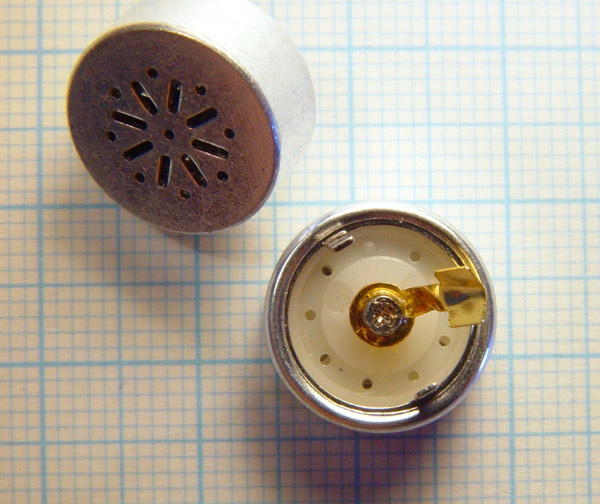
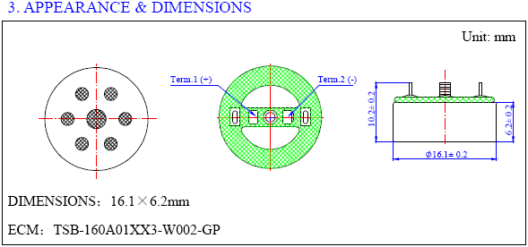
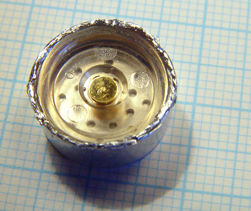
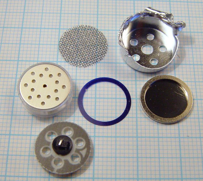
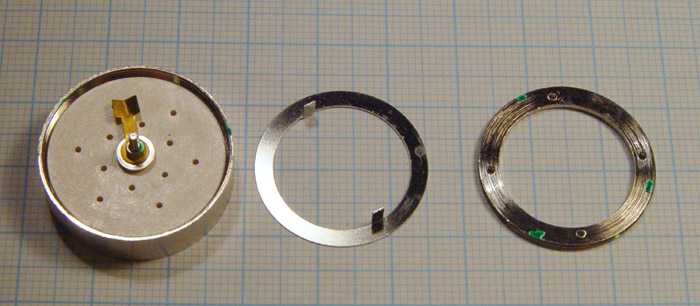
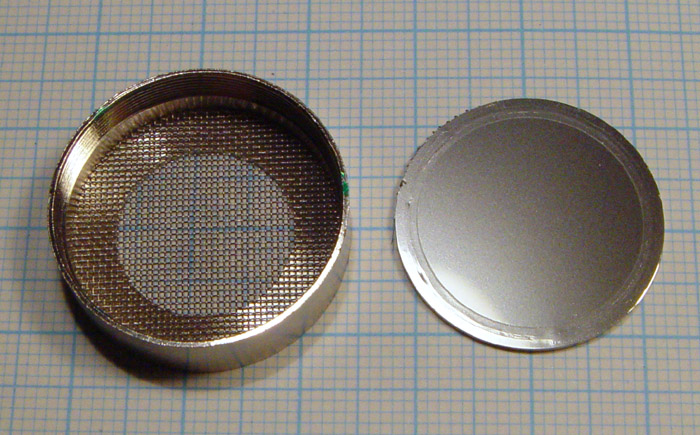
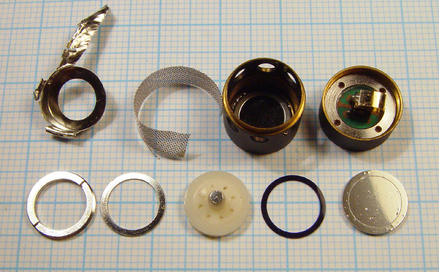
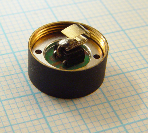
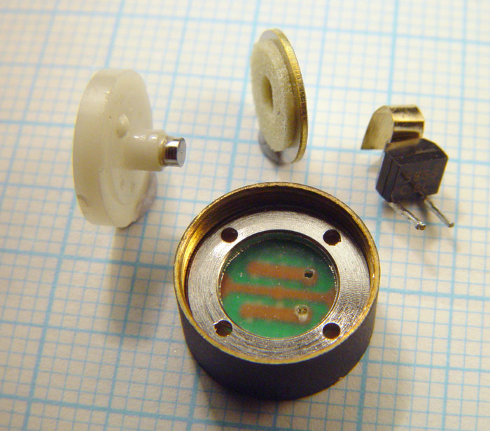
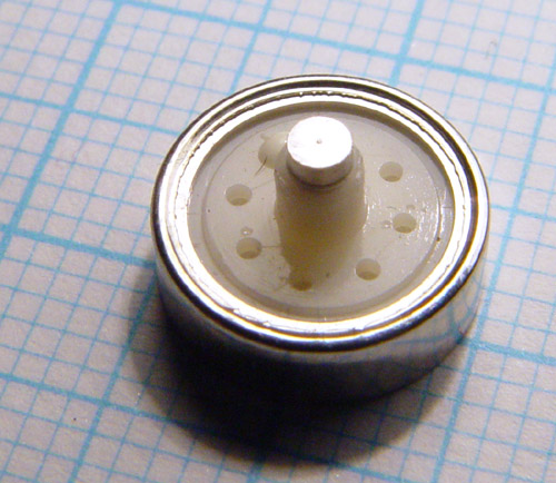
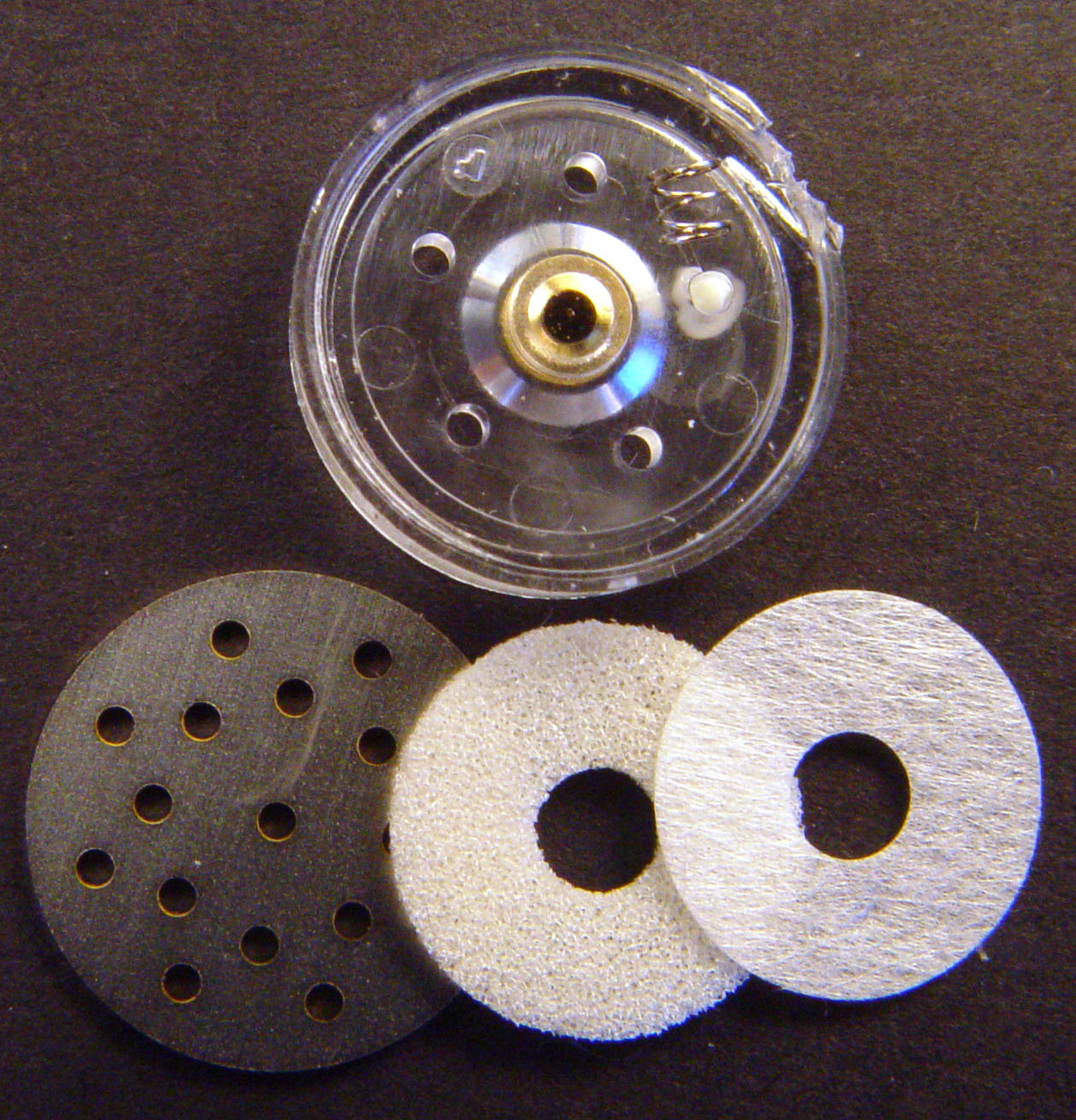
Dismantling the TSB-140AO
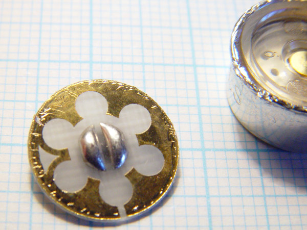
To use the microphone, wires would be
connected to both terminals of the FET and to the gold-plated copper
track on this rear printed circuit board (PCB).
The capsule is sealed at the back in terms of short-term air pressure
variations. Since the crimped aluminium retention of the PCB is
not glued or soldered, air would seep through the gaps between the
aluminium and the PCB. So when there are long-term changes in
atmospheric pressures, the internal air pressure would follow that of
the outside. Without this - if the back was completely sealed -
the diaphragm would be pushed in or out if the internal air pressure
was not the same as that outside.
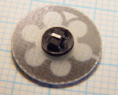
The FET has its gate pressed against a
gold-plated stud in the transparent piece of plastic. The source
and drain are available separately.
Its only identifying marks are a few dots and "J34".
Richard Crowley
of the Micbuilders list told me that this was probably a 2SK1109
N-channel FET, specifically made to be an impedance converter for
electret microphones. Indeed, "J34" is one grade of 2SK1109s:
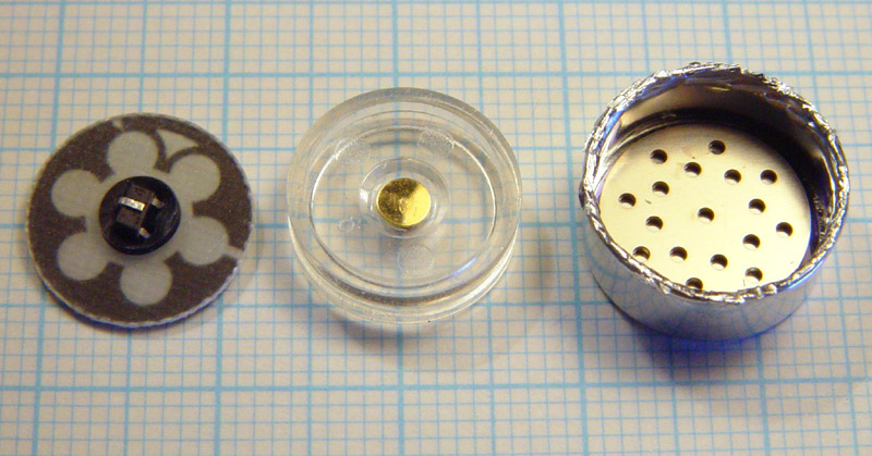
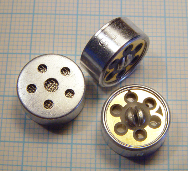
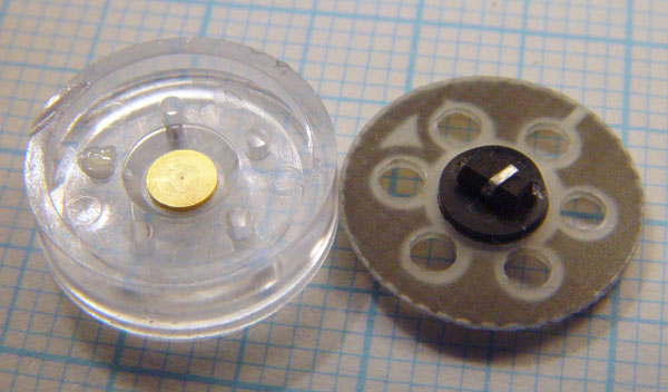
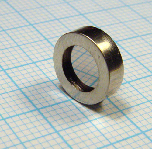
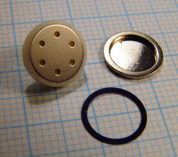
Here we see the transparent piece with
its back towards us and the back of the backplate. The backplate
is brass and is plated with something silvery. The yellow
appearance in this
photo is not realistic.
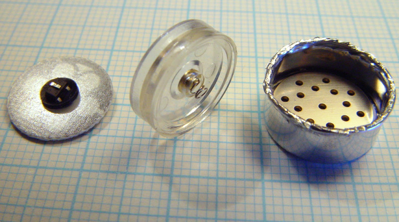
There is a small spring - stainless steel, I guess - which connects the front part of the gold-plated stud to the backplate.
The backplate is 0.53 mm thick and 12.0 mm in diameter.
It is somewhat recessed in the transparent piece, which has an outside
diameter of 13.0 mm, to match the 13.1 mm inside diameter of the
aluminium shell.
The internal diameter of the cavity behind the backplate, which is the main area of the transparent piece visible here, is 10.5 mm. The depth of the cavity, once the backplate is in position, is 0.7 mm.
Some of the volume is taken up by the central part with the gold-plated
stud. Also, there is some extra volume of air in the 17 holes in
the backplate.
This is an omni-directional microphone and there is no damping material
in this cavity. The two other microphones which I dismantled are
directional and have damping material in their cavities.
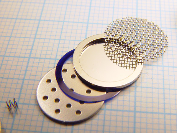
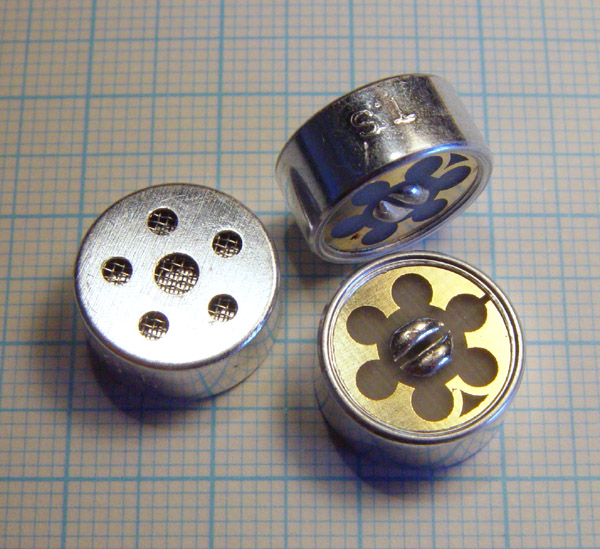
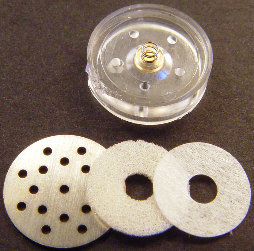
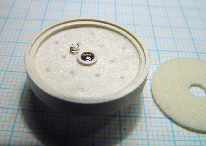
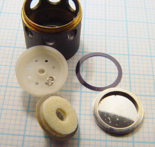
Here we see the components in order
from the front. The grid and then the ring with its diaphragm. The aluminized side is topmost and is visible
here. The other side is the plastic side.
The backplate with its electret layer is pressed up against the
blue spacer ring, which presses against the non-conductive side of the
diaphragm.
The
spacer ring is
60 um thick.
The
diaphragm is
6 um thick.
2009-09-28: Calculating the capacitance
of the diaphragm to backplate system, ignoring the thickness and
capacitance of the diaphragm, and ignoring the holes in the diaphragm:
Area of a 10.5 mm circle = pi * radius
2 = 86.6 mm
2 = 0.000088 square metres.
Gap = 0.00006 metres
Permittivity of air is close enough to the permittivity of free space,
expressed in terms of capacitance = 8.85 pF per meter separation per
square meter.
An online calculator for this is:
The result is 12.8 pF. After allowing for the holes and, I guess
11 pF
or so is a reasonable figure. The backplate would also have a few
pF to ground, around its edges - for instance where it touches the
spacer ring which is pressed against the diaphragm where it is bonded
to its support ring, sideways to the case and back to the case and PCB
via the clear plastic piece.
The two most important dimensions, apart from the diameter of the
active part of the diaphragm: 10.5 mm, and the charge of the electret
film on the front of the backplate are the thickness of the spacer
and the depth of the cavity.
A 0.001 instantaneous increase in air pressure will compress the air in
the cavity and so (in a simplistic view of the motion of the diaphragm)
cause it to move 0.001 x 0.7 mm towards the backplate. This is
0.7 um. This displacement is a significant fraction of the
distance from the back of the diaphragm to the backplate: 0.7 / 60 =
0.012 of the distance. So I can imagine sound pressure at 0.001
of atmospheric pressure causing an instantaneous change of voltage on
the backplate of 0.012 of whatever the effective voltage is on the top
of the electret layer.
Increasing the depth, or the total volume, of the cavity would increase
sensitivity - but potentially lead to resonances. Decreasing the
spacer width would increase sensitivity, but limit the diaphragm's
ability to move towards the backplate without hitting it.
The diaphragm's metalization (I assume it is aluminium) is thin enough
that some light passes through it - I measured about 10%. So it
is possible to see clearly through it when
looking at light fittings, light-globes etc. A similar level of
transparency can be found in aluminized food packaging films. The
diaphragms of the two older Panasonic 9.7 mm omni capsules which I
dismantled had a similar amount of light transmittance. Those
diaphragms were thicker and were electrets.
How does this thin layer of aluminium survive? It is on the front
surface - this can be tested with a multimeter. Aluminium
oxidizes instantly (or very quickly at least) on contact with air,
producing a thin layer of aluminium oxide, which is a ceramic, and
protects against further oxidation.
Hundreds of millions of electret microphones in cell-phones have people
talking into them with moisture, dust, vibration and whatever
else. Yet these electret microphones are extraordinarily reliable.
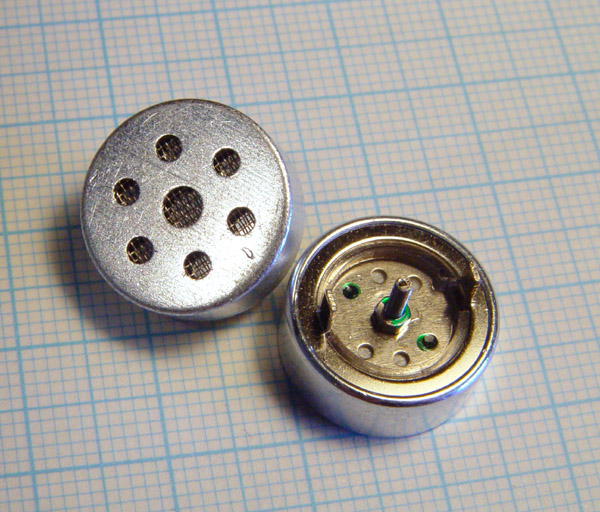
Dismantling the TSB-140A
This capsule appears to be identical to the TSB-140AO except that:
- The clear piece of plastic has some holes in it - five holes, of which one is blocked.
- There are two pieces of damping material in the cavity.
- The PCB has five large holes.
The cavity is the same - 10.5 mm internal diameter and 0.7 mm deep.
The first layer of damping material is some kind of plastic foam, as
described below for the TSB-2555A. This annulus is 10mm
wide. It is about 0.8 mm thick and compresses to about 0.2 mm, or
a little thinner if forced hard.
The second layer is some kind of open-weave synthetic material. It is 100 um thick.
Behind the clear plastic piece a second
cavity is formed between it and the PCB. This is not much of a
cavity, due to the large holes in the PCB, but here are the
measurements.
I estimate the PCB is 2.6 mm behind the rear rim of the clear plastic
piece. The internal diameter of the aluminium case is 13.6
mm. Most of the back of the clear piece is recessed about 1.2 mm
from the rim, so most of the second cavity has a depth of 3.8 mm.
The FET takes up some room and around the edge the depth is less due to
the rim of the clear piece. The inside diameter of this part of
the cavity, due to the rim, is 11.0 mm.
I guess the volume of this second cavity, taking account of the FET and
the rim, when adjusted to the diameter of the active diameter of the
diaphragm (10.5 mm), would be about 3.5 to 3.8 mm.
I will be interested to test these directional cartridges modified to
be an omni by blocking the five holes in the PCB. There would
then be a smaller, damped, first cavity, four small holes and a second
larger cavity. I estimate the effective depth of the first cavity
to be about 0.45 due
to the space taken up by the damping materials. If the rear holes
were
sealed, and the resistance of the four internal holes ignored (which is
not realistic, except at lower frequencies) then in theory the two
treated as a single cavity would have an effective depth of about 4.0
to 4.3 mm, which is about 5 times the effective depth of the single
undamped cavity in the omni version: TSB-140-AO.
I would expect a larger cavity to lead to greater sensitivity, since
for a given air pressure variation, the diaphragm must move more in
order that the pressure in the cavity matches that on the top face of
the diaphragm. However, as the cavity becomes physically larger,
this will be frequency dependent and there may be resonances.
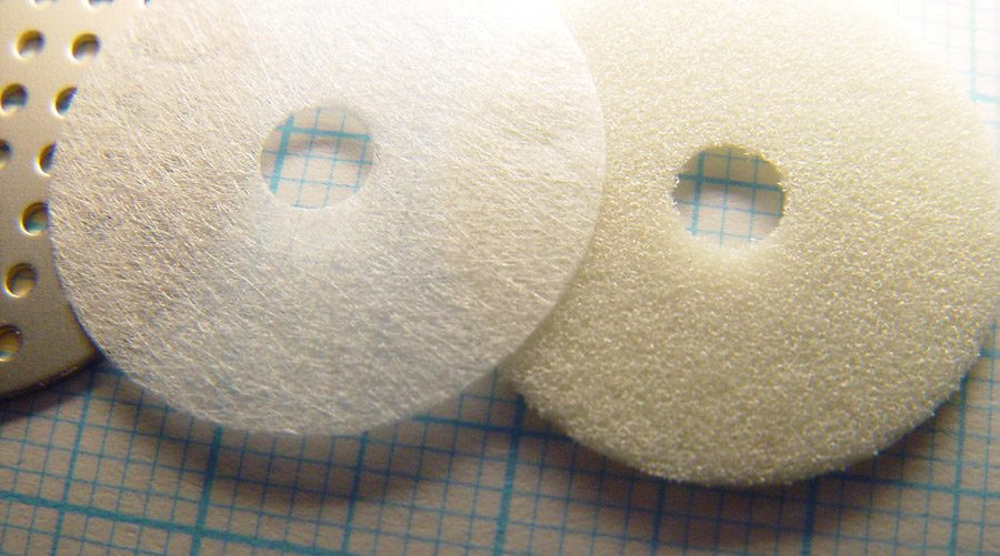
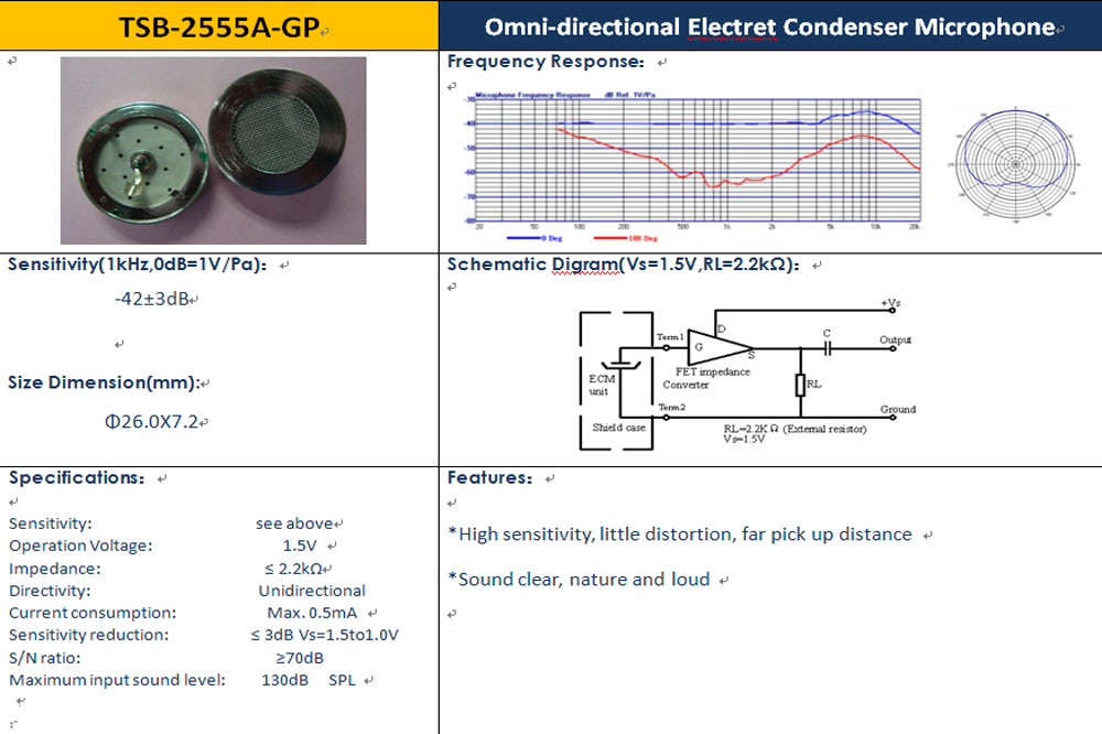
Dismantling the TSB-2555A
This microphone has no FET.
Please see above for the links to the Transsound page in July 2011 for
the current version: TSB-2555A-GP and for the datasheet.
Omni-directional microphones such as the TSB-140AO are pressure sensors.
The cavity behind the diaphragm has no openings to the outside world.
The TSB-2555A is a "unidirectional" microphone, meaning it tends to
sense sound waves coming from the front, but not from
behind. It senses pressure
gradient between its front and back, so it has holes at the back.
It also has two damping materials in its
cavity.
Its main body is based on turned metal - brass I guess - rather than pressed aluminium.
I did not have any special tools for unscrewing the ring via its holes - I
simply used a 1mm drill, some pointy-nosed pliers and a small
vise. First, I used a vise to squeeze around the back of the
case in multiple positions, to break the bonds between the metal ring
and the case. Then I gripped the front of the case in the vise
and levered the drill in order to turn the ring.
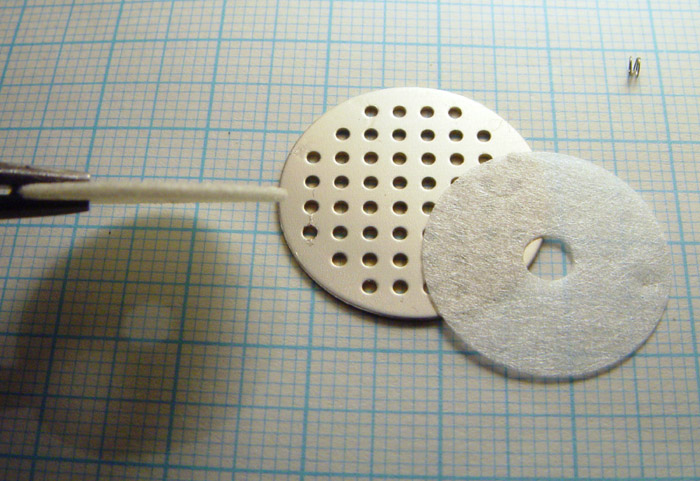
Now we see the white plastic piece,
with the backplate firmly pressed into it. In front of the backplate is
the spacer ring. On the left we see the non-conductive back side of the diaphragm.
On the right, we are looking at the metal of the back-plate, which is
coated in a thin, transparent, not entirely smooth, layer of electret
material. I assume this is Teflon or something similar. It seems
to be slippery like Teflon, but the surface texture is not precisely
flat.
I scraped a little of this from the surface and applied a soldering
iron to it. It softened, I think, but did not melt or burn.
I reckon it is Teflon or some other fluoropolymer film.
I have taken off the spacer ring.
The internal diameter of the spacer ring, which sets the effective diameter of the diaphragm, is 21 mm.
I have dropped out the diaphragm and its ring and placed the diaphragm front (and ring) downwards.
The diameter of the front hole is 16mm.
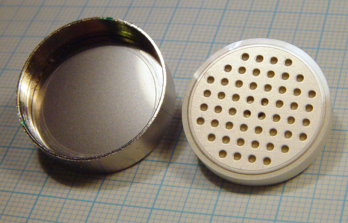
Here we see the front of the three
parts - the case, the diaphragm's metalized side and ring and the front
of the backplate with its associated white plastic piece.
The backplate is plated brass, 0.56 mm thick. The 52 holes are about 1.2 mm diameter.
The
diaphragm is
~6 um thick.
The
spacer ring is
75 um thick.
As for the capacitance calculation for the TSB-140AO above, here us an
estimate for the the capacitance of the diaphragm to the
backplate.
0.000075 metre separation.
21 mm diameter circle has area of 346.3 mm2 , but there are 52 holes each with a diameter of 1.2 mm have an area of 58.8 mm2, so the total area is about 287.5 mm2 = 0.0002875 metre. The result is 3.3925E-11 farad = 34 pF.
The
cavity is
1 mm deep, but is filled with damping materials.
There is a little spring which goes
from the head of what I will call a "screw", since it has a metal
thread protruding out the back of the capsule. There's no need to
loosen the nut, but I did - and then it is hard to tighten it since
the "screw" has no slot.
If this was an omni, there would be no holes in the white plastic
piece. There are 12 holes which cause the entire microphone, to
some extent at least, to measure pressure gradient and therefore be
directional.
The cavity is 1mm deep from the back of the back-plate. However,
this is not free air - it is filled with two discs of dampening
material, both 20 mm wide:
- At the front, a disc of open-cell foam (I guess this is the best
description). This is a foam plastic of some kind, which
can be stretched somewhat, and which has cellular foam where the walls of each
cell are largely open to the next cell. So air can be blown through the disc quite
easily. I can't tell what sort of material this is - though
perhaps I could be burning it with the soldering iron and comparing the
smell with those of other samples burnt the same way.
If it is a polyurethane foam, then I imagine it will turn to sticky
crap at sometime in the future - maybe decades from now. However, there
are many other types of foam which I think are more stable than this.
This foam disc is 0.8 mm thick and can be squashed to 0.2 mm.
When trying to look through this disc at a bright light, it a few
pinholes which appear to let through direct light, but the holes are
too small and/or too few to be able to see an image through.
- At the back of the cavity, a lightweight synthetic random weave
material 80 um thick. This is partially open, since it is
possible to look through it and see the filament of a light-globe.
The holes in the white plastic piece are between 0.8 and 1.0 mm - I guess 0.9 mm.
The combination of the small holes and the damping material (depending
on how the capsule is housed in an external body for the whole
microphone assembly) causes delay and filtering of the sound which
reaches the rear of the diaphragm. This is explained with a
diagram on page 17 of the
above mentioned Neumann microphone handbook.
Dismantling the TSB-120A
I didn't take photos of some earlier
parts of the process. The rear part of the capsule unscrews
easily. This contains the FET, soldered to a small PCB. The FET's
identification markings are:
596S
C 6L
(Not 569S as I previously wrote.)
Eric Benjamin corrected my mistake in reading these numbers. He
informs me that this is a 2SK596 of the 'C' grade: IDSS = 210 to 350
uA. Here's the datasheet:
2SK596-datasheet-Sanyo.pdf .
The two parts of the body are made of turned brass. This is
mechanically quite a complex capsule. I don't understand how it
would screw into anything while making electrical contact at the same
time, without soldered wires.
After the back part has been removed, a
small ring with two slots can be unscrewed and the inner cartridge
removed. This is 10mm in diameter:
The body is not aluminium - it is a
thin metal such as steel, however it is not magnetic. It may be
brass, but if so, it must be a very light yellow colour.
There are 8 holes. One of them is blocked with white material. I
think the holes are about 0.5 mm in diameter and that they are about
0.5 mm deep.
Here are all the parts after I had almost completely dismantled the inner capsule:
Just inside the seven holes in the front there is a piece of black synthetic random-weave material.
Above is the electret-layer front of
the backplate, the spacer ring (75 um thick) and the diaphragm and its
ring. I think I can measure the thickness of the diaphragm with
an accuracy of +/- 1 um, and my measurements suggest it is 3 um thick.
The backplate pops off easily.
There is a small spring connecting it to the conical front end of the
plated metal stud in the middle of the white piece of plastic.
There is an annulus of foam material which looks similar to that in the
TSB-2555A. It is about 0.7 mm thick when not compressed and about
0.2 mm thick when squashed.
There was also an annulus of white random-weave material at the back of
the cavity. As I prised it out with a needle, it sprung away and
is still AWOL somewhere in my workshop.
The cavity is about 7.5 mm wide and about 0.7 mm deep.
There is a lot of careful turning,
painting and assembly in this microphone. I think this is quite
remarkable for a product which sells for USD$6.20 in quantities of 100
or more.
This is the only one of these microphones I bought, so I won't be able to test it.
The TSB-120A has been discussed on the Micbuilders list. Searching for it at:
turns up various discussions.
Detecting the electret charge without electronics
While I was sure that the three
Transsound microphones I dismantled were back electrets, and the two
older Panasonic 9.7 mm omni capsules I dismantled were "foil type" or
"charged diaphragm type", I wanted to see the elecret's effects
directly.
Here are two techniques which worked fine for me.
Firstly, the front surfaces of the Transsound backplates and the back surfaces of the Panasonic
diaphragms all picked up cornstarch and ordinary wheat flour.
The second test was more satisfying. I cut a strip of kitchen
aluminium foil (10 um thick) 70 mm long and 2 mm wide. I
suspended this so one end hung free. I grounding the top end of
the
foil by touching it with a finger of my left hand. Then I held
the Transsound backplate or the ring of the Panasonic diaphragm
with pointy-nose pliers in my right hand. With a finger I touched
the metal of the pliers. This ensures the alfoil strip has the
same voltage (presumably zero, unless I am charged) as the metal of the
backplate or the aluminized side of the Panasonic diaphragm. (I
found it not good enough to use a strand of hair or even a strip of
paper, since these could develop static charges of their own.)
I could attract
the dangling tip of the foil strip with the electret layer. The
attraction was only visible at a range of less than 1mm, but once the
foil came close, the force was stronger and it tended to stick to the
electret layer.
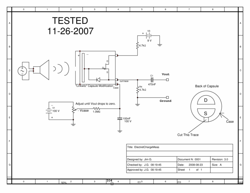
Measuring the electret layer's voltage (electret polarization voltage)
Addition on 2011-07-04, following discussions on the Micbuilders list around 2011-05-19:
It may be interesting to measure the voltage imposed by the electret
layer. We can think of it like a capacitor with a certain voltage
across it, in series with the backplate, but with no metal conductive
"plate" on the front surface of the electret layer.
To
measure the voltage of the
electret layer, it is necessary to have a mic capsule with direct
access to the backplate. This is assuming the electret layer is
on the front of the backplate, as it is in the capsules mentioned on
this page.
However, here is a diagram of measuring the polarization voltage of a capsule which has an internal FET:
http://i114.photobucket.com/albums/n253/zapnspark/ElectretChargeMeas.png
This "Linkwitz modification" is for internal FET microphones where the
source of the FET is connected to the body of the microphone, and
therefore the diaphragm. The modification (if it is possible)
involves cutting the connection between the drain terminal and the body
of the microphone. Ordinary 2 terminal electret mics with
internal FETs need to be modified to achieve this. Whether or not
it is possible depends on the exact details of the microphone.
I think this page:
http://www.linkwitzlab.com/sys_test.htm#Mic is the original page describing what has become known as the "Linkwitz mod".
The TSB-140 pictured above already has independent connections for the
source and drain of the FET, so there's no modification required.
The current production TSB-140A25-GP also has separate connections for
drain and source: D = terminal 1, S = terminal 2. Unfortunately,
the datasheet doesn't mention which is terminal 1 and 2! Terminal
2 is the larger of the three, which is clearly connected to the body of
the microphone. However, it probably makes little difference,
depending on the amplifier configuration, to use the source instead of
the drain and vice-versa.
G is the gate, which goes to the backplate. The triangle which
represents the FET is erroneous in that it has a fourth unlabeled
terminal going to the body of the microphone (the diaphragm). I
am sure there is no such connection. The FET has a gate, a source
and a drain. There's no fourth terminal or need to connect any
part of the FET to the body of the microphone.
There needs to be a very high impedance amplifier, located very close
to the backplate, since its capacitance to the diaphragm is
small. This could be a FET or MOSFET input op-amp, or a FET-based
amplifier of some other kind.
By altering the voltage between the backplate and the diaphragm (the
diaphragm is normally grounded) we will be able to find a voltage at
which the diaphragm's voltage is the same as that of the front surface
of the electret layer. When this is the case, there will be no
electrical signal in response to sound moving the diaphragm.
One way to do this would be to keep the diaphragm and so the body of
the microphone at 0 volts, and to alter the backplate voltage.
This would typically require a low-leakage capacitor between the
backplate and the FET/MOSFET buffer amplifier. In that case, I
suggest watching out for leakage or other discharges which could damage
the buffer amplifier. The voltage of the diaphragm needs to be
set via a high value resistor. I guess 10 or 100 megohms would be
fine. We are not trying to built a full-range microphone - so if
the low-frequency response is cut by this, that's fine - just use a
5kHz test sound.
Another way would be to keep the backplate directly connected to the
FET buffer and to alter the voltage of the diaphragm, and so the body
of the microphone. Again, there could be leakage currents due to
the high voltages involved (I guess 50 to 100 volts - I haven't tried
this). So diode protection of the buffer amplifier would be a
good idea.
In either case, to really be sure of the voltage on the backplate, it
would be best to measure the current going through the 10M or 100M
resistor, or to in some other way establish the actual voltage of the
backplate. (Of course, if you are using a 1:1 voltage buffer such
as can easily be made with a MOSFET op-amp, then you already know the
backplate voltage with great accuracy, since the offset voltage of the
op-amp will be small compared to the voltage you are interposing
between the backplate and the diaphragm.)
If you kept the diaphragm at 0 volts and used a capacitor to couple the
backplate to the buffer amp, with a (say) 10 meg resistor driving a
variable voltage (say +/- 100 volts) to the backplate, then if you
could establish that the current going through the 10M resistor was
quite low, then there would only be a volt or so across this resistor -
so you know the backplate voltage quite accurately. Another
approach, if you use a higher value resistor and can't measure the
current through it, would be to touch the backplate to a second test
voltage, and watch the output of the buffer amp. When the second
test voltage exactly equals the actual backplate voltage, there will be
no change in the output of the buffer amp.
Search engine bait with misspellings: transound microphone
transound electret transsound mics transsound electret microphones.
~~~ooo000ooo~~~