How do modern high-end routers implement the
Fowarding Information Base function?
This
page is a sidebar to the page in the parent directory, concerning
SRAM-based forwarding and a LISP-like protocol for achieving
multihoming and traffic engineering.
Robin Whittle rw@firstpr.com.au 2007-04-20 (minor update 2007-07-25 - price of CRS1 MSC card)
To the
main
page on SRAM-based IP forwarding
The
sections below discuss how the FIB function - AKA "route lookup"
function is performed on a number of high-end routers. A summary
is at the parent page ../#FIB_techniques .
Does the FIB usually involve
TCAM?
When
I wrote the I-D (to version 01) I understood that a typical approach
for router design was to use TCAM (Ternary Content Addressable Memory)
to implement the FIB function: throwing the destination address into
the TCAM would produce a number of the first matching TCAM line, which
then becomes the address of an SRAM, which reads out some previously
written data which tells the router which interface to forward the
packet to. There are many papers referring to the use of TCAM
for this "longest prefix match" operation, such as
Fast
incremental updates on Ternary-CAMs for routing lookups and packet
classification by Devavrat Shah Pankaj Gupta, Feb 2001.
See also the Force 10 and Cisco presentations linked to below
#Cisco_others_TCAM .
The lecture notes by Prof. Zhi-Li Zhang's
csci5221-router-design.ppt
(PowerPoint, early 2007) documents various approaches, including the
RAM-based "Recursive Flow Classification" (RFC). These notes
include:
Putting a small cache of the FIB on each line card, with the central CPU handling packets which miss the cache (p42).
125 million packets a second is needed for 40Gbps (p 47).
Cost, speed and power consumption of DRAM, SRAM and TCAM - 15 to30 watts in 2003/04 (p 48).
Explanation of binary tries, path-compressed trees, multi-bit tries etc.
Explanation of TCAM and other techniques.
Here is a quote from page 96:
Lookup: What's Used Out There?
Overwhelming majority of routers:- modifications of multi-bit tries (h/w optimized trie algorithms)
- DRAM (sometimes SRAM) based, large number of routes (>0.25M)
- parallelism required for speed/storage becomes an issue
Others mostly TCAM based:
- for smaller number of routes (256K)
- used more frequently in L2/L3 switches
- power and cost main bottlenecks
So on this basis,
most high-end routers do no use TCAM. Maybe they already have enough memory to map every IPv4 /24 as I suggest.
knew some routers, including especially those from
Juniper, used other techniques. I was told by two people with
long experience in this field that TCAM is
not
normally used (for instance in Cisco routers) for the FIB function.
But I think TCAM is widely used, although the latest, highest
capacity routers from Cisco and Juniper use an ASIC with external
DRAM or SRAM. It is these newer, core and edge routers which are important to this discussion.
Juniper documentation (
Efficient
Scaling for Multiservice Networks
page 6) indicates TCAM is typically used (in other company's routers)
for filtering, but that filtering in Juniper routers is performed by
similar techniques to those used for "route lookups". These
techniques are tree-based, as depicted on page 9.
Juniper's
M120 and MX960 do not seem to use TCAM for any function.
Both of these use a single, very large - and indeed heroic -
chip
called the I-Chip to process packets, including rewriting them and
deciding which interface to forward them to, via a separate switching
system. The I-Chip integrates the function of 10 ASICs in earlier
Juniper products and uses external high speed RAM. Multiple reads
of
this RAM are used to traverse some kind of radix tree or trie. I
guess this RAM would also store data for handling MPLS too. More
on
packet
classification algorithms and on the memory in Juniper routers below.
Some
Cisco routers certainly do use TCAM. The CRS-1 does not seem to
use TCAM - I think it uses and ASIC and DRAM or SRAM.
Juniper M120 uses RLDRAM
A Juniper/Micron case
study
download.micron.com/pdf/case_study/juniper.pdf
from 2006 states that Juniper chose RLDRAM-II (as described
below)
in their M120 router which was announced in mid-2006. The
separate input and output pin version is used, in the 288 Mbit size.
This is the first of their routers to use the I-chip.
The
second is the larger MX960. Scrutinising the documentation, I
see
there is 64 Mbytes of RLDRAM in the Forwarding Engine Board, of which
there are up to 6 in each router. (
M120
Internet Router Hardware Guide
page 156.) RLDRAM-II with 288 Mbits are 9, 18 or 36 bit wide
devices. They are also available in 8, 16 and 32 bit
versions,
which are 32 Mbytes each. So that means there must be two of
these chips on each Forwarding Engine Board (FEB). The board
also
has 512 Mbytes of slower DDR DRAM, which is probably largely visible in
the drawing (p19) as 3 x 4 small devices (there would be 4 x 4 on the board) to the left of the big
heatsink, which presumably cools the I-Chip.
According to the case-study RLDRAM-II
was
chosen because it was much faster than DDR DRAM. A 15ns
latency
is quoted, compared to 55ns for DDR. Also, RLDRAM-II was
significantly cheaper and denser (bits per chip) than DDR-II SRAM or
QDR-II SRAM. Assuming the 72Mbit QDR-II SRAMs were available
at
design time, there would need to be 8 QDR-II SRAM chips instead of 2
similarly mechanically sized RLDRAM-II chips.
So
it seems
that some routers do have enough high-speed RAM to implement the direct
lookup of 24 bits of IPv4 which I am proposing. However,
I am not sure how much of this 64Mbytes is used for buffering packets.
It seems the RAM would be kept busy with lookups and the
like, so
maybe buffering is on the I-Chip. The only other RAM is
slower
DDR DRAM for the main CPU and for buffering. Page 85 shows 512Mbytes of DRAM, with 63% devoted to buffering.
The line cards (FPC and cFPC) have DRAM which is used largely for
buffering - page 83 shows them with 128Mbytes of DRAM, with ~58% used
for buffering.
I guess the
I-Chip would be flexible enough to use 24 bits of the IPv4 destination
address to look into a table in RAM. My single 72Mbit
QDR-II SRAM proposal is for 16 Mbytes (actually 8M x 9, but used as 16M
x 4 for routers with less than 14 interfaces.) The high
speed RAM in the M120 is needed for a variety of purposes, but
it
doesn't seem impossible that an eighth or a quarter of this
(14.5M x 4 bits for less than 14 interfaces or 14.5Mbytes
for up
to 254 interfaces) could be devoted to IPv4 forwarding on /24
boundaries. I imagine a significant rewrite of the operating
system and microcode of the I-Chip would be required to do this.
This shows
that the cost of the memory I am proposing to add is not prohibitive.
Each of these two 288Mbit RLDRAM-II chips would probably cost
as
much, or more, than the 72Mbit QDR-II SRAM I propose using.
I
see a
retail
price
(April 2007) for the M120 FEB is USD$18,992.44. So the $70
cost
of the memory I am proposing ($140 for larger routers, and less in the future) is unlikely to be a major concern.
The power dissipation of the FEB is rated at 86
watts (p
203), so the additional 1 to 1.4 watts for the memory chip I am
proposing (2 to 2.8 watts for larger routers) is also unlikely to be a major concern.
Further
description of the M120 architecture can be found in
Integrating
Ethernet in Converged Networks
. The
M120 has up to 6 boards (4 x FPC and 2 x cFPC, all on the front of the
router) for driving Ethernet links etc. each operating at up to 10Gbps
duplex. There are up to 6 FEBs at the rear of the router, and
each one can be selected to handle the packets being received from one
cFPC or from two type 1 FPCs. Exceedingly fast serial links
are used
on the
midplane, and one FEB can be a spare, reconfigured automatically in
less than a second, depending on the arrangement of FPCs and FEBs
There are various websites which state that the CPU
(presumably
the I-Chip) on the FEB is 667MHz, but I can't find this at the Juniper
site.
Juniper MX960 uses SRAM?
Juniper's
second router to use the I-Chip is the MX960. The I-Chip
resides
directly on the Dense Port Concentrator (DPC) boards, into which
individual PIC boards are plugged, to provide a total of 40Gbps of
Ethernet etc. links. (This means there is no failsafe
swapability
of forwarding logic as with the M120.) There is no mention
of
RLDRAM by Micron regarding the MX960, which was released 6 months or so
after the M120, in late 2006 or early 2007. The Juniper
documentation mentions RLDRAM in the SCB (switch fabric board), but not
the DPC board.
The
Dense
Port Concentrator Guide mentions:
- 335 or 310
watts, depending on the model.
- Total of 40Gbps full
duplex Ethernet capacity.
- MTU 9192 bytes.
Page 81 of the
MX960
Hardware Guide
indicates that each DPC has 256Mbytes of SRAM, which is separate from
the DRAM for the CPU (1024Mbyte). Since they are not using
RLDRAM, and since each DPC board handles 40Gbps full duplex, compared
to the 10Gbps full duplex of each M120 FEB, I guess that they are using
either DDR-II SRAM or QDR-II SRAM, both of which are much faster than
RLDRAM. (However, see the statement linked to
below where a Juniper engineer
states they use DRAM in the MX960.) Do they use one I-Chip or two
or more sharing the
load, each with its own SRAM? In
Integrating
Ethernet in Converged Networks
(page 5) Juniper states that the I-Chip is a 10Gbps packet forwarding
engine, so maybe they use four of them in each DPC. The chip
is
said to be capable of coping with huge scaling, including in the number
of routes, without hardware upgrade. (Page 6.) Maybe they use
four I-Chips, each with 64Mbytes of RAM - the same as used for the M120.
My
guess is that the MX960
uses the same, or similar QDR-II SRAM chips to the one I am suggesting,
but probably uses 32 such chips. In April 2007, the largest
capacity SRAMs are QDR-II or DDR-II SRAMs, with 72 or 64 Mbits.
I
guess that the MX960 could be programmed by Juniper to
perform the SRAM forwarding functions I describe.
Traditional RAM-based approaches
to packet classification AKA "route lookup"
Juniper, in
Efficient
Scaling for Multiservice Networks,
especially page 11, provides an overview of how their routers
process incoming packets. The "tree lookup primitive" is a
low-level function within the system. The "IP Forwarding
Table"
is a body of data in memory and is referred to as the FIB (Forwarding
Information Base). The tree lookup primitive navigates this
tree,
depending on the packet's destination address, and the result is the
selection of the next step in the process: the packet being sent to
whichever interface was specified in the final part of the tree,
perhaps with a filtering stage before it is sent there.
(Also,
the tree lookup could lead to the packet being dropped, I guess.)
Perhaps they cache recent results in the chip, using a hash index into
the cache, to speed up classification.
There
are many types of
classification, but what I am interested in is the FIB function: given
a destination address, determine whether to drop the packet or which
interface to forward it to.
EZchip has a document
"The Role of Memory in NPU Design" at
www.ezchip.com/html/tech_whitepapers.html
. This discusses three approaches to "look-ups".
Firstly,
a direct lookup involves taking N bits of address and using this as in
index (AKA a "key") into a linear list of data which specifies what to
do next. They say this is typically only done for N <=
16.
My IPv4 SRAM-forwarding proposal involves doing it for N=24.
A second approach is to hash a larger
number P of bits into a small enough number Q to use as an index to a
list of 2
Q
variable length lists. Since multiple input values could hash to the
same smaller value, each list of more than one entry must be searched
to see which one applies to the actual input bits. This would be
computationally intensive, since the algorithm somehow needs to look at
all Q bits and somehow determine which of multiple entries in this
table corresponds to this pattern. I don't have a clear idea of
how hashing works efficiently when used to find which of multiple
prefixes a particular 32 bit value falls within. I can imagine it
being efficient when trying to match the address with a moderate number
of single IP addresses, but not with prefixes which span thousands or
millions of IP addresses.
If
the list has no members (its starting address is 0), our lookup ended with no result. If
the
list has one entry, this is the correct one. If it has two or
more (a "hash collision"), we have to somehow look at the original 32
bits and the individual list items to determine which list item
corresponds to the actual input bits. This is messy, but it
is
potentially faster than a tree based approach, as described below, and
its memory requirements may be practical, whereas implementing a list
of 2
32 items is generally prohibitive.
(Though iPods have 4Gbytes of FLASH memory . . . )
EZchip
state they can preform hash lookups with no more than two memory
lookups. This sounds pretty impressive - I can't imagine how they do it - but it would depend
on
the nature of the bits being processed and how many rules are encoded
by the system.
The EZchip paper gives a rough
description of a
tree or trie based approach. More detailed descriptions of hash and trie
approaches can be found at:
www.cs.mcgill.ca/~cs535/lect_notes/Lecture14-RouterArchitectures.pdf .
The simplest approach,
with the most
compact utilisation of memory, involves stepping through the tree one
bit at a time. This is way too slow for handling 24 or more
bits
of address information with 10Gbps interfaces. Stepping 16
ways,
on 4 bits at a time, is faster, but leads to larger memory
requirements. The fastest way to handle 24 bits is to use
them as
an index into RAM - which is what my IPv4 proposal entails. See the parent page for a
reference to where this was first suggested in 1998 by Nick McKeown and colleagues.
EZchip
states that by stepping multiple bits per cycle, they cut the number of
cycles required by about a third. So I assume they are
stepping 3
bits at a time. In practice, with an IPv4 FIB, it makes sense
to
do bits 31 to 24 bits in one cycle, since there are no rules for
prefixes shorter than /8. This still leaves 16 bits or more
to
handle. EZchip state that by doing some of the tree lookups
using
memory inside their Network Processor Unit chip, and leaving the rest
to external RAM, they can speed things up considerably. I haven't figured out how this could be practical.
Cisco CRS-1 - FIB
implemented with ASIC and RAM?
Below
#Cisco_Catalyst_6500_FIB
I point to Cisco presentations and documentation which shows that they
use TCAM for the FIB in at least some of their routers, notably the
Catalyst 6500. Here I discuss what little I could find out
about
the FIB function in the CRS-1 - but after writing this, I found a paper
which describes the Tree-Bitmap alogorithm, which is apparently used in
the CRS:
../#Vargese_CRS_1 .
The CRS-1 has an
ingress FIB and
an egress FIB. It is the former we are interested in, because
this uses the destination address of an IPv4 or IPv6 packet to
determine which interface the packet should be forwarded to.
One
of the various System Description documents, such as:
Cisco
CRS-1 Carrier Routing System 16-Slot Line Card Chassis System
Description,
describes the Modular Services Card (MSC). Each MSC connects
to
its own PLIM card, which provides the Ethernet etc. interfaces to the
outside world. Page 5-6 has a drawing.
The
Ingress
Packet Engine
is shown on page 5-3. One of its functions is to "Perform an
algorithm to determine the appropriate output interface to which to
route the data.". This document says nothing more about the
Ingress Packet Engine, but it does state the MSC's power consumption is
375 watts. It handles 40Gbps (full-duplex - a total data rate
of
80Gbps) and is a lot heftier and no-doubt more expensive than Juniper's
10Gbps USD$19k M120 Forwarding Engine Board. Update 2007-07-25:
sure enough, the list price of a CRS-MSC is USD$80,000, as shown
here ,
here and
here.
The
best information I could find on the CRS-1's Ingress FIB is from
Advances
in Routing Architecture : The CRS-1 and IOS-XR , by Andy
Chien from March 2005. From this, I ascertain:
- The
Ingress Packet Engine is here referred to as the "RX SPP (Silicon
Packet Processor) L3 engine".
This ASIC is fabricated with IBM's Cu-11 process (a
130nm process using copper for conductors, rather than
aluminium).
- The chip contains 188 32-bit CPUs
running at 250MHz.
Packets are distributed to these CPUs and their output is muxed
together. All CPUs access external off-chip memories for the
following functions, referring to four blocks, each of which is
presumably a different kind of "memory" chip, according to page 16:
- ACLs,
Netflow, policing etc. use a 512k entry TCAM - block name "TCAM".
- 2 million entries for IPv4/IPv6/Multicast/MPLS:
two blocks labeled "PLU"
(Packet Lookup, for the FIB, I guess) and "TLU" (Tunnel Look Up, for
MPLS, I guess).
- 1 million 64 bit counters, in
another block labeled "STATS".
I
can't find any information on what chips are used for the "PLU" system.
Are they TCAM with associated SRAM? Are they fast
RAM with
the individual CPUs or some ASIC function doing a trie-style sequence
of accesses? Is there some kind of caching? There
is no
mention of the size or technology of this functional block. I
suspect it is one of the ASICs created by IBM. Is it a fully
self-contained ASIC or an ASIC with external RAM. I suspect the
latter, because of the first line of quoted text here:
The
data
sheet states that the MSC's memory is:
"Configurable
with 2GB of route table memory.
1 GB of packet
buffer memory per side (2 GB total per line card [ingress and
egress])."
I
don't know what "configurable" means (I guess in the next paragraph),
but 2Gbytes is too much to be on an ASIC. It would also be a very
large amount of TCAM - many heatsinked chips. It may be too much to
implement with SRAM. If it is DRAM, then how do they handle
40Gbps of packets (I guess 300 million packets a second at maximum, or
more likely a practical figure of 100 million packets a second) with
DRAM? Even RLDRAM has a long recovery time - such as 15nsec -
before the same block of memory can be used for another read or write
cycle. SRAM has no such problems - it can read or write 250
million cycles per second.
Could the TLU device for handling
MPLS packets may well have on-chip DRAM? For each interface (and
the MSC could be handling 40, I think) there needs to be 2 million
locations, one for each possible MPLS label value. Each location
would have the next hop MPLS entry (21 bits) and probably some bits to
tell the router which interface to send the relabeled packet to.
This sounds like too much, so I would expect external RLDRAM or
SRAM for the TLU. Perhaps the TLU and PLU functions are
implemented on the one chip, with the one amount of memory . . . then,
there would be a
configurable amount devoted to MPLS and the rest available for IPv4 and IPv6 route lookup.
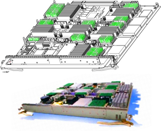
Here
are some images of the MSC board. These are modified Cisco
images. The first highlights the area with vertical mounted DIMMs
or similar, containing presumably DRAM or SRAM. (TCAM would
require heatsinks.) The second is a colour enhanced image, which
shows these green vertical boards more clearly. The big heatsinks
of the major ASICs are visible next to these areas of RAM. I am
not suggesting we try to divine something meaningful from these - I
just like to see the physicality of this important board. Can
anyone send me a better photo? The blocks on the far right are
heatsinks for the power regulators.
IBM's
June 2004
press
release
about the ASICs used for Cisco's CRS-1 states that the SPP is an 18.3mm
square chip (this is BIG, by any standards) - the worlds most
sophisticated ASIC. 185 million transistors, 38 million gates.
This is the largest of 10 chips for Cisco. I wonder
whether
one of the other chips was the "PLU" route lookup "memory"
device. IBM's photo gallery has a
picture
of the SPP chip, with the 188 32-bit CPUs visible.
Unfortunately
the image is not as clear as other close-ups of chips which use similar
technology
here
and
here.
These are multi-megabyte JPGs, shown small on the web page, but
worth downloading and viewing with a proper editing or viewing program,
with zoom.
The multiple levels of copper interconnect are shown
here.
Cisco Catalyst 6500 and other routers' FIB implemented with TCAM
www.nanog.org/mtg-0702/jaeggli.html
This leads to presentations and a
report,
from February 2007. The report indicates that the
Juniper MX960 uses DRAM, rather
than the SRAM which I suggested
above.
"In
the case of Cisco that means delivering switch routers with a capacity
of about a million routes now. In the case of Foundry they
are
projecting that with some FIB aggregation techniques that switches
capable of 512k FIB entries will still be usable by 2014.
Juniper
is delivering new products (M120 MX960) with DRAM rather than TCAM/SRAM
based FIBs with capacities on the order of 2 million ipv4
routes
and they have no reason to expect that they couldn't deliver 10 million
route FIB products in a few years given sufficient demand."
However,
which router manufacturer is going to stand up and say "we can't cope
with the future . . . ". If they are going to do 10 million
routes in IPv6, I think they might as well directly map every /24 as I
suggest, which is 14.5 million.
Greg Hankin's (
Force 10)
presentation
shows the TCAM -> SRAM arrangement for FIB functions.
"Using current 18Mbit
CAMs we can store:
512K IPv4 entries (36 bits for
prefix and mask)
128K IPv6 entries (144 Bits for
prefix and mask)"
This
is one of the reasons my I-D refers to TCAM as a method of performing
the FIB function, with the alternative being ASIC logic and RAM, to do it via a tree search,
as Juniper does. Another reason I wrote that TCAM was often used is the next presentation:
Suran de Silva's (Cisco)
presentation
states that the Catalyst 6500 uses multiple TCAMs. There are
diagrams and photos of the board, with the four FIB TCAMs under
the largest
heatsink. There are
separate
TCAMs for FIB and Access Control List (ACL) filtering.
Most of this Cisco presentation concerns
FIB
TCAM.